Original Link: https://www.anandtech.com/show/15156/imagination-announces-a-series-gpu-architecture
Imagination Announces A-Series GPU Architecture: "Most Important Launch in 15 Years"
by Andrei Frumusanu on December 2, 2019 8:00 PM EST
There are very few companies in the world able to claim a history in the graphics market dating back to the “golden age” of the 90’s. Among the handful of survivors of that era are of course NVIDIA and AMD (formerly ATI), but there is also Imagination Technologies. The company has been around since the early days of graphics accelerators and has seen a shifting industry. In the early to mid-2000’s the company moved away from the desktop space, instead focusing on offering GPU IP optimized for mobile devices.
The Mobile GPU IP Market Situation
The mobile GPU IP market these days is a quite barren landscape; Imagination’s long history along with Arm’s rise to a leadership position with the Mali GPUs has essentially created a duopoly, as smaller vendors such as Vivante have exited the market. The problem of duopolies like these is that there’s a risk of stagnation if either vendor falls behind in terms of technology, and most of the time this comes at the cost of the vendors who rely on licensing the IP.
Over the last several years in particular, we’ve seen a larger shift in the mobile market dynamics as Qualcomm has increasingly managed to dominate over its competitors. The more vertically integrated company produces its own SoC designs using its own in-house GPU IP, and as a result isn’t reliant on technologies from Imagination or Arm (CPUs are a whole other story).
More recently, we’ve seen Apple’s custom GPU efforts make huge leaps in performance and efficiency. While officially we have no concrete information on the behind-the-scenes details of Apple’s design, it’s commonly regarded as a design forked-off from Imagination IP back in 2015, which Apple continues to independently develop thanks to an architectural license. The relationship between Apple and Imagination nowadays is still quite unclear, but the frictions from back in 2017, which ultimately lead to Imagination putting itself to sale and being bought by an equity firm with Chinese investors, seem to have calmed down.
The more important situation to consider is that the two leading GPUs in the mobile market today – Apple and Qualcomm – are designs that are internally developed by the SoC vendors themselves. This is a bit troubling for everybody else in the market, as their reliance on IP licensing means they’re limited in what they’re able to do. MediaTek had suffered quite a lot in terms of market share versus Qualcomm for example (GPU being only one of many other reasons). Other vendors such as Samsung have evidently also realized their situation, and launched development of their own internal GPU architectures, with a more recent surprise development of actually licensing new GPU IP from AMD in order to compete with Apple’s designs.
Introducing Imagination's new A-Series: "Fastest GPU IP ever created"
With that quite long foreword and context in mind, we come full circle to Imagination as well as today’s announcement. Today, the company is revealing its new A-Series GPU IP, describing the new product as Imagination’s most important GPU and IP launch in 15 years. The wording here is extremely strong, and the goals of the new product seem pretty clear: reverse the trend of market share loss against custom GPUs in the market, and put licensed GPU IP back at the forefront of performance.
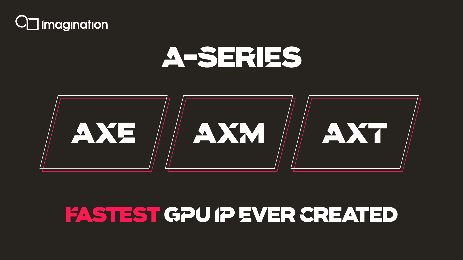
A-Series is the company’s 10th generation GPU architecture and represents a big leap for the company. Even something simple, like the product names, have changed. Gone is the longstanding PowerVR branding, in favor of a more immediate focus on Imagination the company. We'll still see PowerVR around – Imagination is keeping it to describe their technology, particularly their tile-based deferred rendering approach – but after over 20 years it's no longer a brand in and of itself.
As a note on the new GPU IP naming scheme: it’s a deliberate departure from the numerical numbering of the past, and instead is trying to represent a new clean start going forward. I asked, but unfortunately the name it isn’t meant to be a clever twist on a “Series 10” with the numbering now represented in hexadecimal, a pity I say!
The new naming crosses the company’s whole GPU range going from the low-end, mid-range to high-end. Here we see the continuation of the XE, XM and XT suffixes; however as in the past, there are architectural differences between the IPs, with today’s news mostly covering the new XT series.
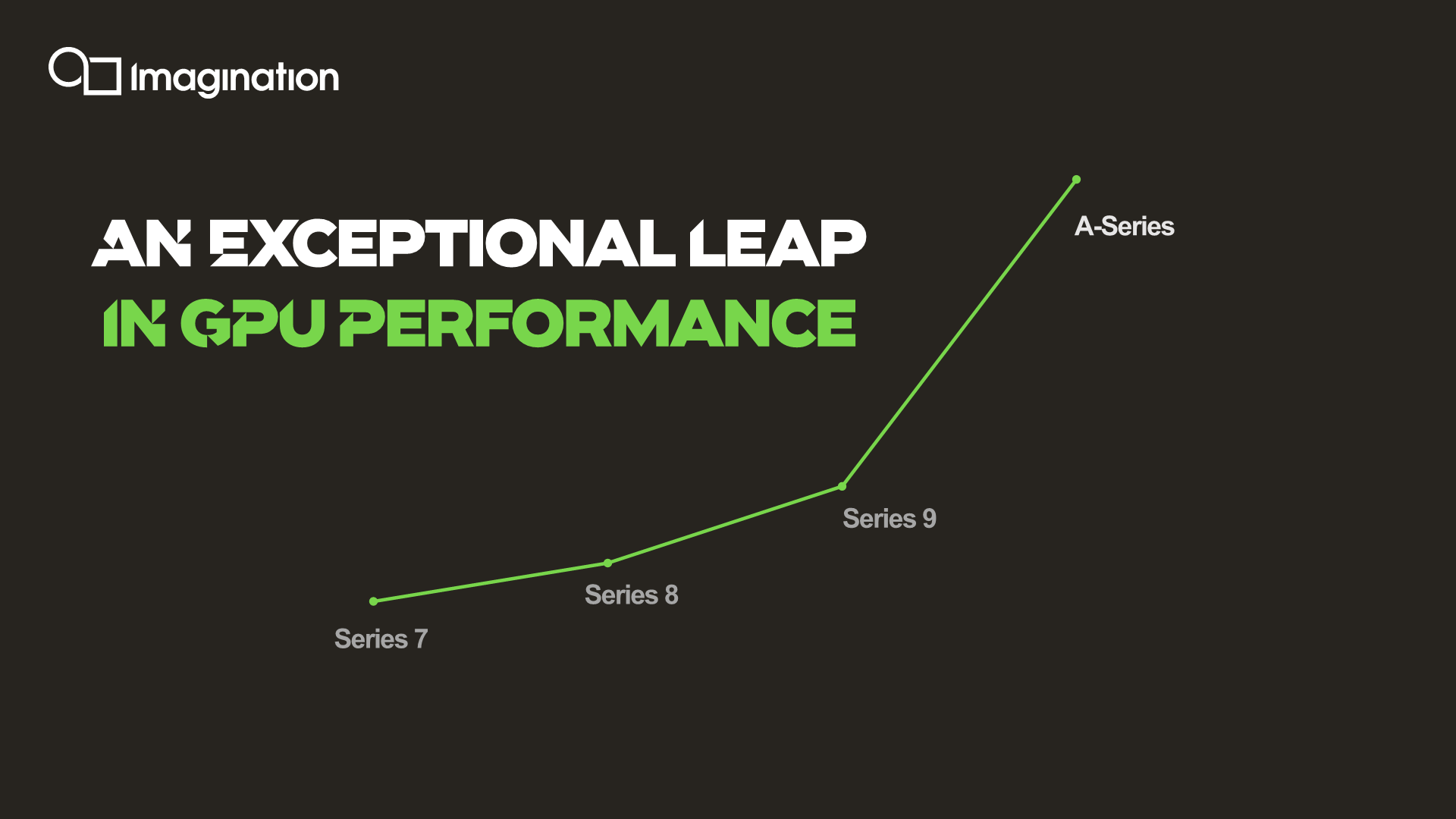
As mentioned, the new A-Series promises to bring some exceptional leaps in performance compared to past generation designs, although it’s also important to point out some footnotes on the matter.

An important metric that’s been showcased today is Imagination's claim that the new A-series XT design is 2.5x faster. "Fast than what" you might ask? The figure represents the new architecture’s performance leap in an ISO-area and process node comparison against Imagination's previous generation Series 9 GPU.
The thing to note is that the company isn’t doing exact apples-to-apples comparisons between different generations of XT GPUs, but rather is making comparisons to the latest widely available “Series 9” on the market. This was an unfortunate, but yet practical choice to make given that currently there’s no publicly announced or available chips which make use of the company’s 8XT or 9XTP designs.
The comparison data here is likely based on MediaTek’s Helio P90 with the GM9446 – technically part of the 9-series, but also architecturally based on the older Rogue architecture. Imagination wanted to be more transparent in regards to its area and performance claims for the A-Series, and the comparison with the 9XM Rogue-based GPU provides a much more recent and readily available baseline against which vendors can independently verify and compare metrics to.
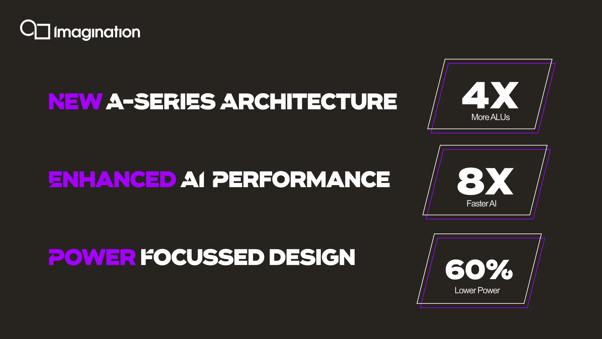
Key improvements of the A-Series include a massive overhaul over the GPU’s compute units and ALU architecture, promising a 4x increase over a 9XM Rogue GPU. AI is a first-class citizen in the A-Series and we’ll be seeing dedicated compute resources resulting into improvements of up to 8x in performance. Finally, the new architecture is said to bring a very large leap in terms of power efficiency, with the new design consuming 60% less power for a similar level of performance.
The new architecture covered today spans four disclosed configurations in the XT series, as well as one XM configuration. The XE series, while having seen improvements, isn’t based on the new architecture, but rather a continuation from the previous generation.
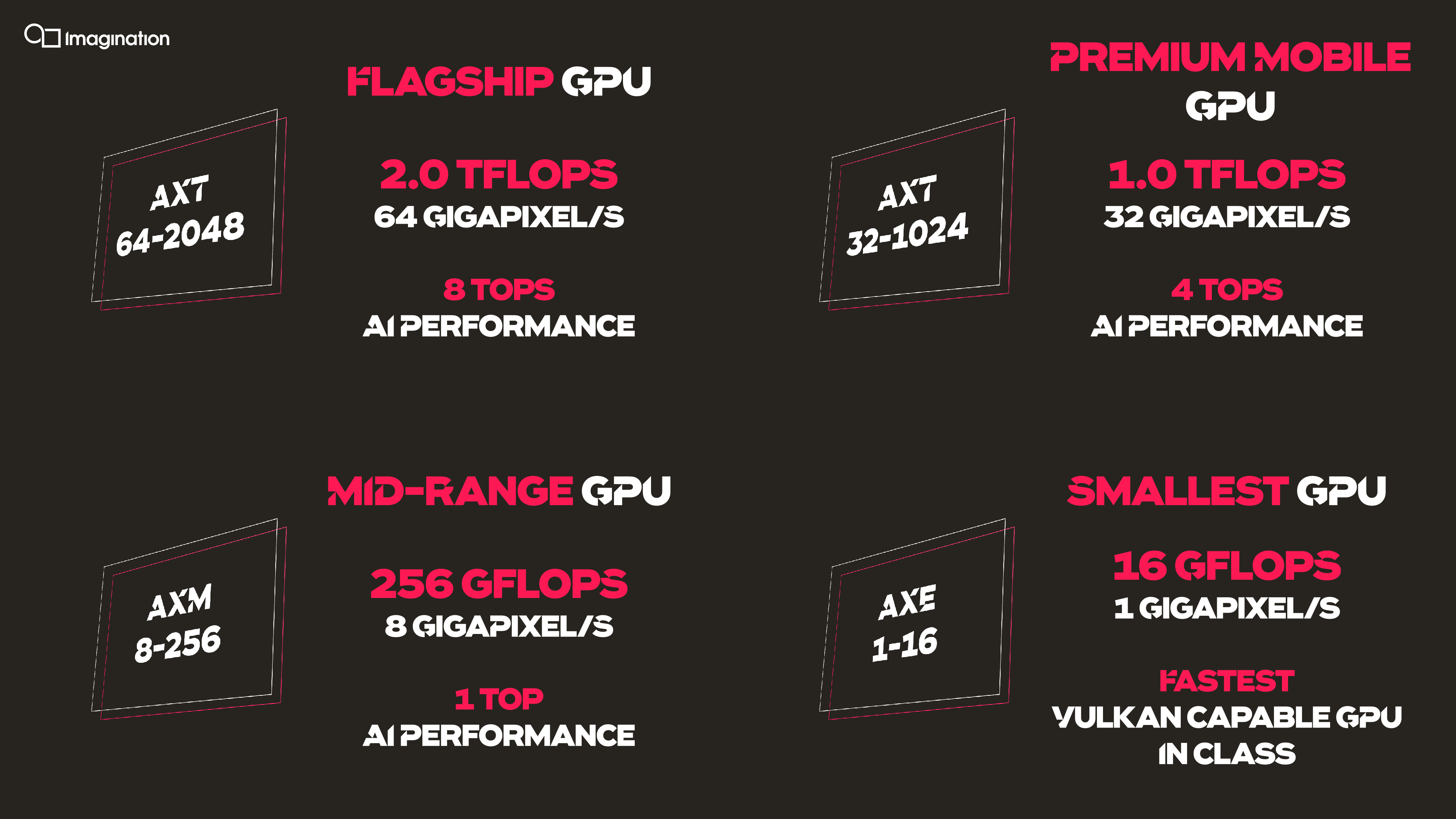
Imagination’s naming for the new A-Series is extremely straightforward in regards to understanding their positioning a performance. The AXT-64-2048 for example represents the highest end configuration of the architecture in the XT range, achieving 64 texels per clock and 2048 FP32 FLOPs per clock. AI TOP performance is quadruple the FLOPS, so in this case for an envisioned 1GHz design, the AXT-64-2048 reaches 2 TFLOPs in graphics and compute power, 8 TOPs in INT8 inference throughput, and 64 Gigatexel/s fill rate.
It should also be noted that it's more correct to say Gigatexels/s instead of Gigapixels/s as in the marketing materials published - Imagination found that a lot of people didn't correctly grasp the meaning of texture fillrate and thus opted to simplify the marketing information in pixels/s.
The figures scale down the range with corresponding performance with the AXT-48-1536, AXT-32-1024, AXT-16-512 and finally the AXM-8-256. The AXE-1-16 is a separate, smaller more customized microarchitecture.
Imagination envisions the AXT-32-1024 to be the traditional sweet-spot target for a premium mobile GPU SoC in smartphones, while the larger configurations would possibly be used in larger form-factor devices.
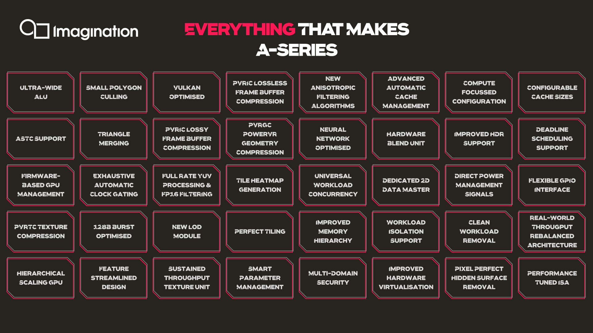
The company calls the A-Series “the GPU of everything”, and there’s indeed a ton of changes and features that make up the new IP. We’ll be covering a few aspects of the company’s disclosed big matrix of features above, starting off with one of the biggest changes, the GPU’s ALU architecture.
New ISA & ALUs: An Extremely Wide Architecture
As mentioned, the ALU architecture as well as ISA of the new A-Series is fundamentally different to past Imagination GPUs, and in fact is very different from any other publicly disclosed design.
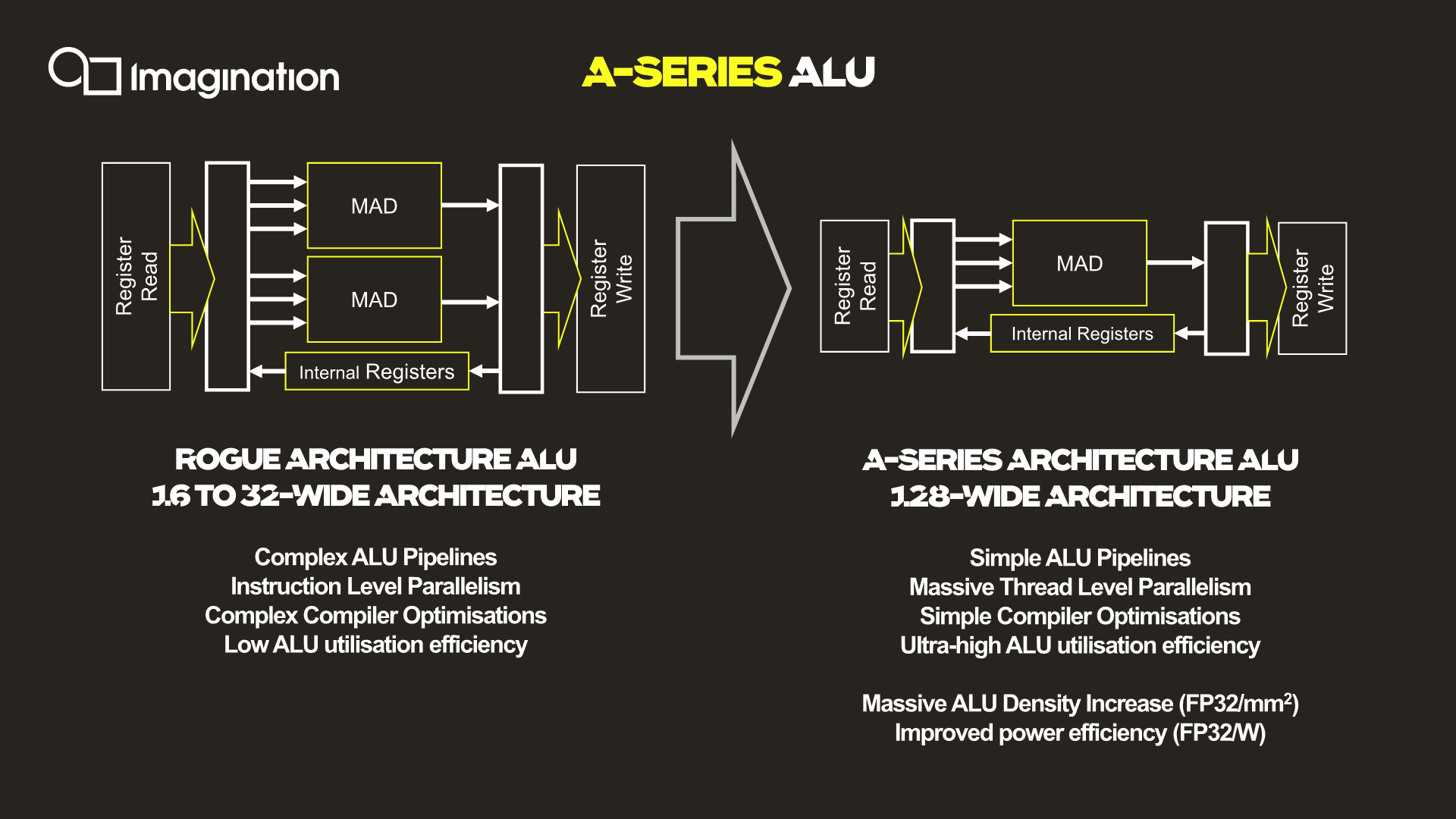
The key characteristic of the new ALU design is the fact that it’s now significantly wider than what was employed on the Rogue and Furian architectures, going to up a width of 128 execution units per cluster.
For context, the Rogue architecture used 32 thread wide wavefronts, but a single SIMD was only 16 slots wide. As a result, Rogue required two cycles to completely execute a 32-wide wavefront. This was physically widened to 32-wide SIMDs in the 8XT Furian series, executing a 32-wide wavefront in a single cycle, and was again increased to 40-wide SIMDs in the 9XTP series.
In terms of competing architectures, NVIDIA’s desktop GPUs have been 32-wide for several generations now, while AMD more recently moved from a 4x16 ALU configuration with a 64-wide wavefront to native 32-wide SIMDs and waves (with the backwards compatibility option to cluster together two ALU clusters/CUs for a 64-wide wavefront).
More relevant to Imagination’s mobile market, Arm’s recent GPU releases also have increased the width of their SIMDs, with the data paths increasing from 4 units in the G72, to 2x4 units in the G76 (8-wide wave / warp), to finally a bigger more contemporary 16-wide design with matching wavefront in the upcoming Mali-G77.
So immediately one might see Imagination’s new A-Series GPU significantly standing out from the crowd in terms of its core ALU architecture, having the widest SIMD design that we know of.
All of that said, we're a bit surprised to see Imagination use such a wide design. The problem with very wide SIMD designs is that you have to bundle together a very large number of threads in order to keep all of the hardware's execution units busy. To solve this conundrum, a key design change of the A-Series is the vast simplification of the ISA and the ALUs themselves.
Compared to the Rogue architecture as depicted in the slides, the new A-Series simplifies a execution unit from two Multiply-Add (MADD) units to only a single MADD unit. This change was actually effected in the Series-8 and Series-9 Furian architectures, however those designs still kept a secondary MUL unit alongside the MADD, which the A-Series now also does without.
The slide’s depiction of three arrows going into the MADD unit represents the three register sources for an operation, two for the multiply, and one for the addition. This is a change and an additional multiply register source compared to the Furian architecture’s MADD unit ISA.
In essence, Imagination has doubled-down on the transition from an Instruction Level Parallelism (ILP) oriented design to maximizing Thread Level Parallelism(TLP). In this respect it's quite similar to what AMD did with their GCN architecture early this decade, where they went from an ILP-heavy design to an architecture almost entirely bound by TLP.
The shift to “massive” TLP along with the much higher ALU utilization due to the simplified instructions is said to have enormously improved the density of the individual ALUs, with “massive” increases in performance/mm². Naturally, reduced area as well as elimination of redundant transistors also brings with itself an increase in power efficiency.
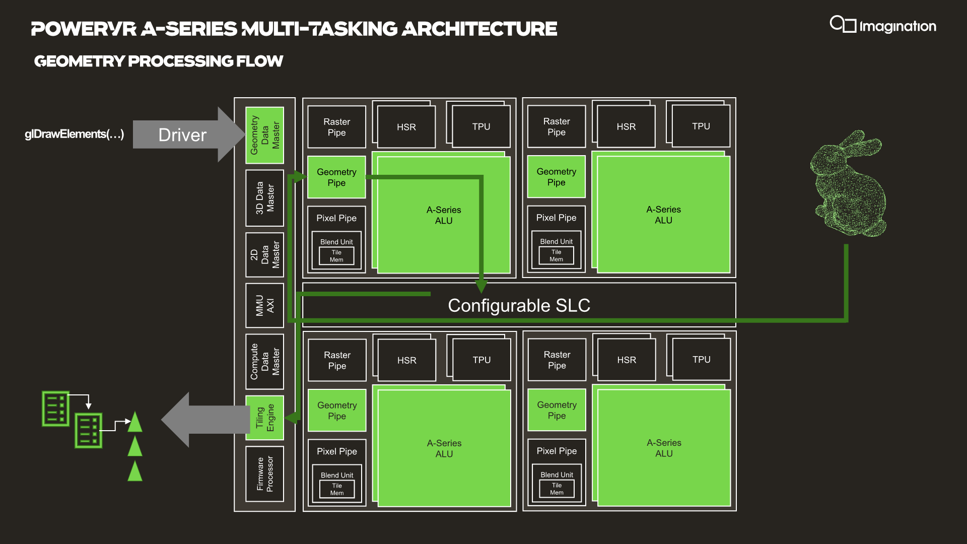
The next graphic describes the data and execution flow in the shader processor.
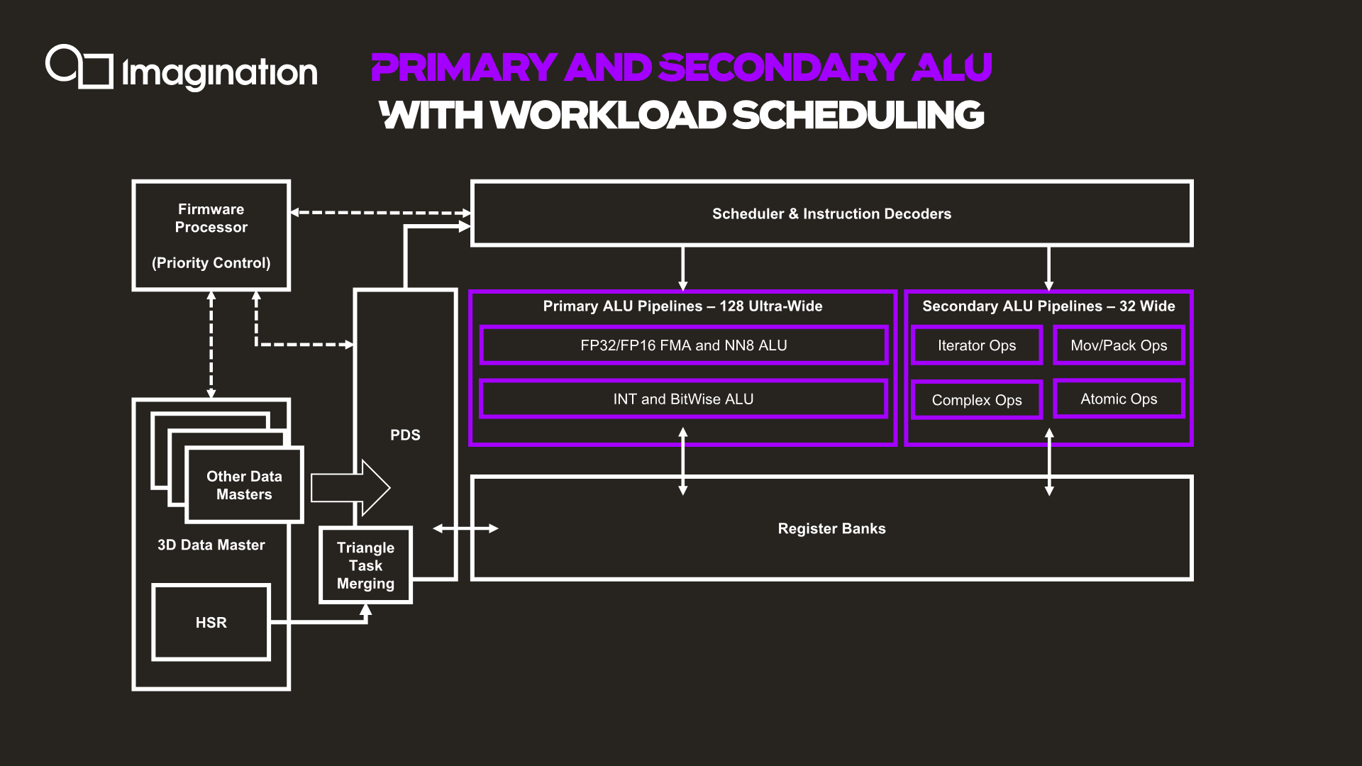
Things start off with a data master which kicks off work based on command queues in the memory. The 3D data master here also handles other fixed-function pre-processing, which will trigger execution of per-tile hidden surface removal and workload generation for the shader programs. The GPU here has a notion of triangle merging which groups them together into tasks in order to get better utilization of the ALUs and able to fill the 128 slots of the wavefront.
The PDS (Programmable Data Sequencer) is an allocator for resources and manager. It reserves register space for workloads and manages tasks as they’re being allocated to thread slots. The PDS is able to prefetch/preload data to local memory for upcoming threads, upon availability of the data of a thread, this becomes an active slot and is dispatched and decoded to the execution units by the instruction scheduler and decoder.
Besides the primary ALU pipeline we described earlier, there’s a secondary ALU as well. First off, a clarification on the primary ALUs is that we also find a separate execution unit for integer and bitwise operations. These units, while separate in their execution, do share the same data paths with the floating-point units, so it’s only ever possible to use one or the other. These integer units are what enable the A-Series to have high AI compute capabilities, having quad-rate INT8 throughput. In a sense, this is very similar to Arm’s NN abilities on the G76 and G77 for integer dot-product instructions, although Imagination doesn’t go into much detail on what exactly is possible.
The secondary pipeline runs at quarter rate speed, thus executing 32 threads per cycle in parallel. Here we find the more complex instructions which are more optimally executed on dedicated units, such as transcendentals, varying operations and iterators, data conversions, data moving ops as well as atomic operations.
Fixed Function Changes & Scalability
Zooming out from the ALU, we’re seeing a higher-level block configuration that’s very similar to past Imagination PowerVR GPUs. The ALUs themselves are still housed in the larger cluster block that’s called the USC, or unified shading cluster. The USC along with various other fixed function blocks is in turn housed in an SPU, or shader processing unit, effectively the scaling block regularly referred to as a “core”.
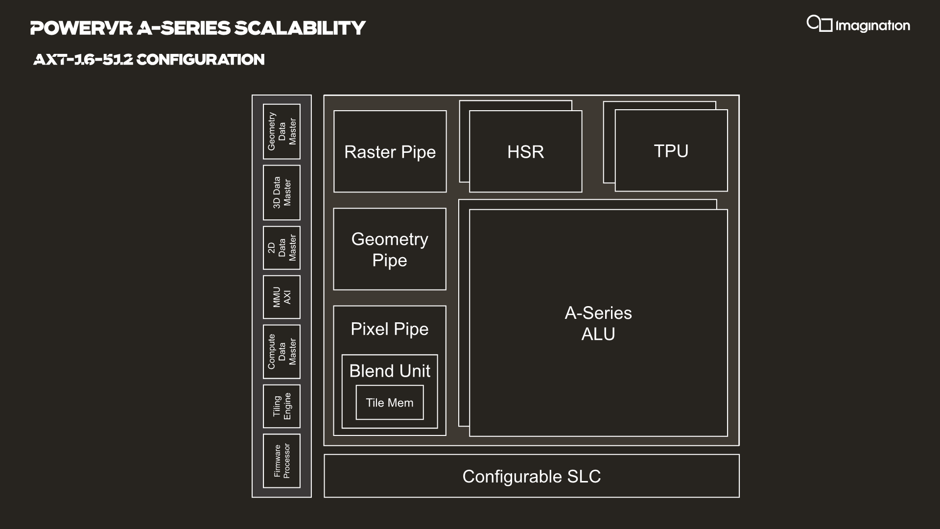
Each SPU houses two USCs in the current IP configuration, meaning we have two clusters of 128-wide ALUs. This is valid for all AXT parts, but we imagine the AXM-8-256 unit just has a single USC. The AXT-16-512 is the smallest configuration with a fully populated SPU.
Each SPU has its own geometry pipeline, and up to two texture processing units. The A-Series carries over the per-TPU throughput design from the Furian architecture, meaning the block is able to sample 8 bilinear filtered texels per clock. The A-Series doubles this up now per SPU and the AXT models feature two TPUs, bringing up the total texture fillrate to 16 samples per clock per SPU.
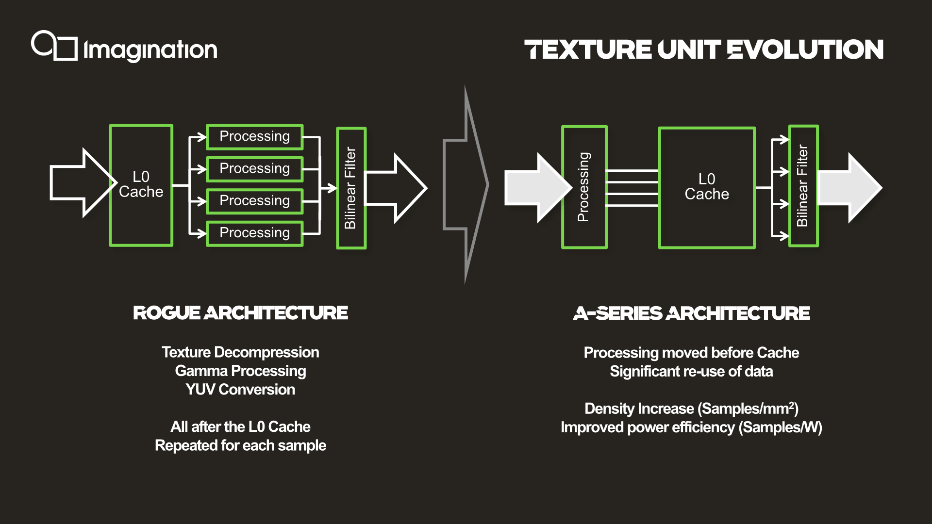
The microarchitecture of the texture units has also evolved beyond just their throughput. A bigger improvement that Imagination is disclosing is the handling and location of the L0 cache. The L0 cache has been relocated within the texturing workflow to between the processing and filtering stages, allowing the L0 cache to hold the outputs of the processing stage, rather than the inputs. This allows for what Imagination calls significant data reuse, as texels don't need to be re-processed each time they're needed. And given how many times a texel may need to be sampled during anisotropic filtering, it's easy to see why. With the benefit of hindsight, this seems like an obvious improvement to make, but the company says that the design choices of the legacy configuration made sense at the time of conception and the workloads back then.
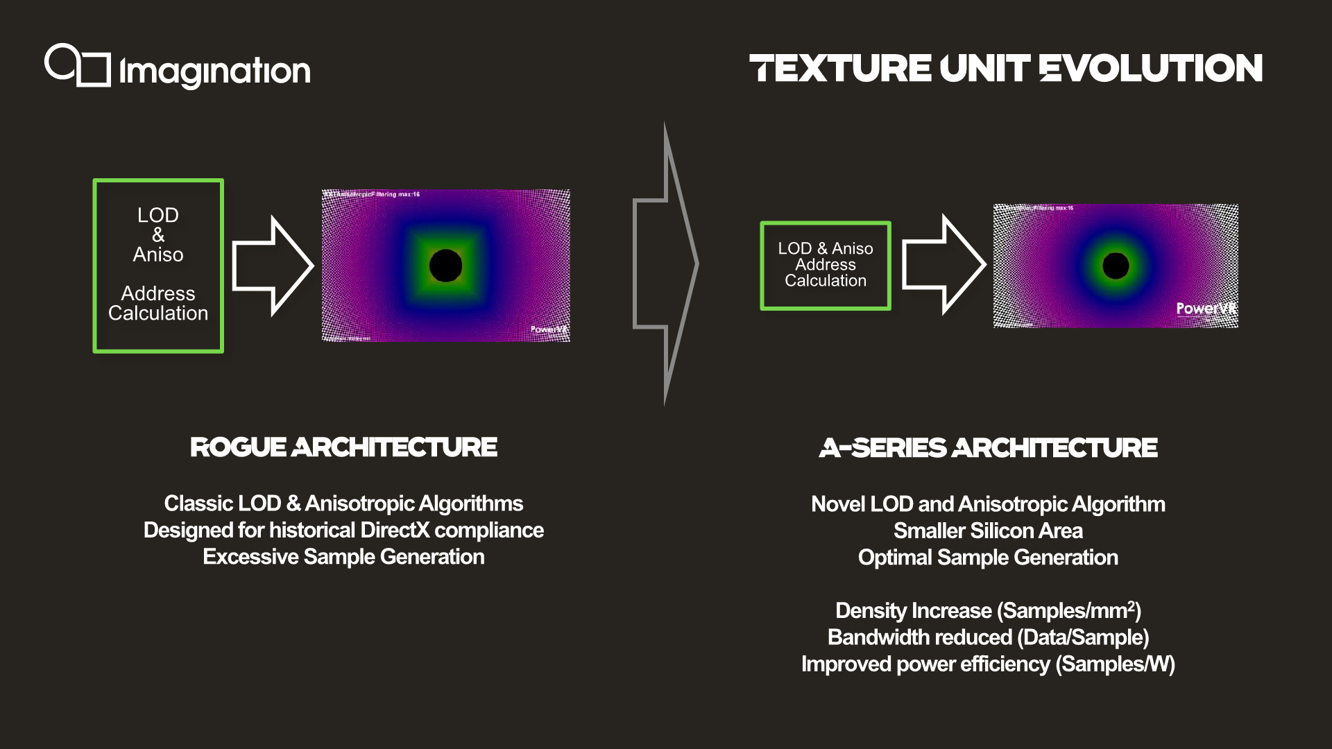
Imagination also talks about how the anisotropic filtering quality of the new architecture is much improved. In a set of comparison screenshots using a traditional texture tunnel, Imagination is showcasing that its new anisotropic filtering algorithms are far closer to being angle-independent – the ideal outcome for aniso filtering – as opposed to angle-dependent filtering with rather hard 90 degree angles on Rogue. Interestingly, Imagination is claiming that they've achieved this improved angle-independence even with fewer fewer samples, all of which serves to improve their efficiency and hardware density. With all of that said, since the comparison is against the Rogue architecture, I’m not entirely sure if it’s an actual novelty of the A-Series or rather a rehash of the anisotropic improvements that already got introduced in the 9XM series last year.
Another change in the fixed function units is found in the pixel pipeline, although superficially the throughput here doesn’t change compared to what we’ve seen on Furian. There’s still up to two PBEs with throughputs of up to 4 pixels per clock, and the design houses two such units for a total of 8 pixels per clock per SPU. There’s actually more internal distinction of the units though – at the front and back core it’s still able to handle 16 pixels per clock and also blend at 16 pixels per clock, although it’s limited on write out to 8 PPC on 1:1 pixel:texture situations.
Imagination’s doubling of the texture throughput whilst maintaining a steady pixel throughput means that the company is generally matching the decreasing pixel:texel fillrate throughput ratio we’ve also seen in other architectures such as from Qualcomm as well as the new Mali-G77, and now falls in at a 1:2 pixel:texel for the A-series.
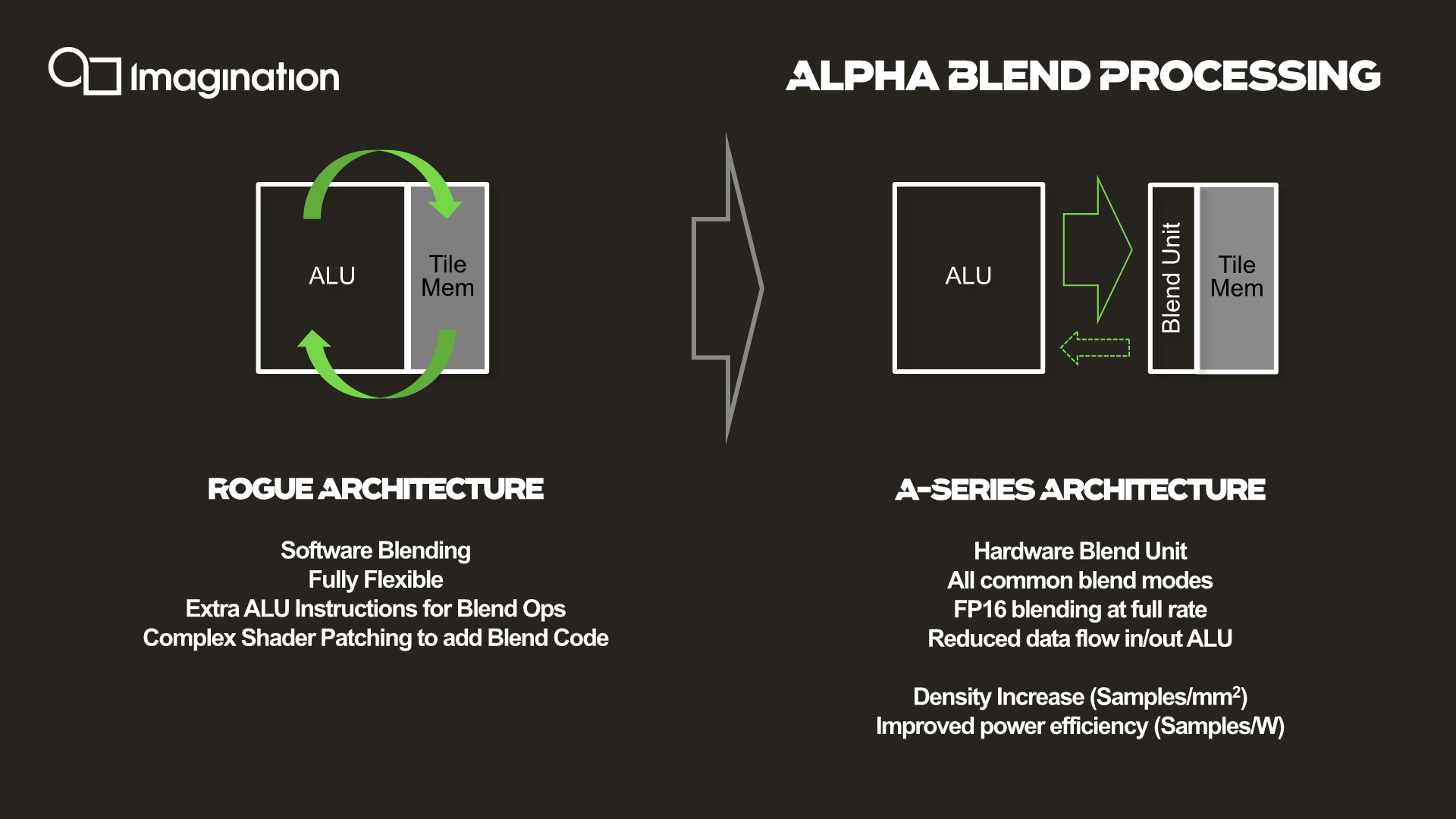
Alpha blending is now done on a dedicated hardware unit in the pixel pipeline instead of being computed by the ALUs. The change results in higher performance through the use of fixed function hardware, allowing for things such as FP16 blending at full rate, and frees up the ALUs themselves so that they can use their computation resources on other work. Density is improved, but more importantly it’s also improving power efficiency as it’s avoiding using more expensive and less task-specific hardware for the same tasks.
It’s to be noted that for the AXM series, the company uses customized fixed function units that are more area efficient, rather than just only scaling the numbers of units.
Scaling Things Up
With the SPU being the coarsest scaling block of the architecture, Imagination is building larger GPU configurations by simply adding in more SPUs. Essentially this is the “core” scaling of Imagination's GPU designs.
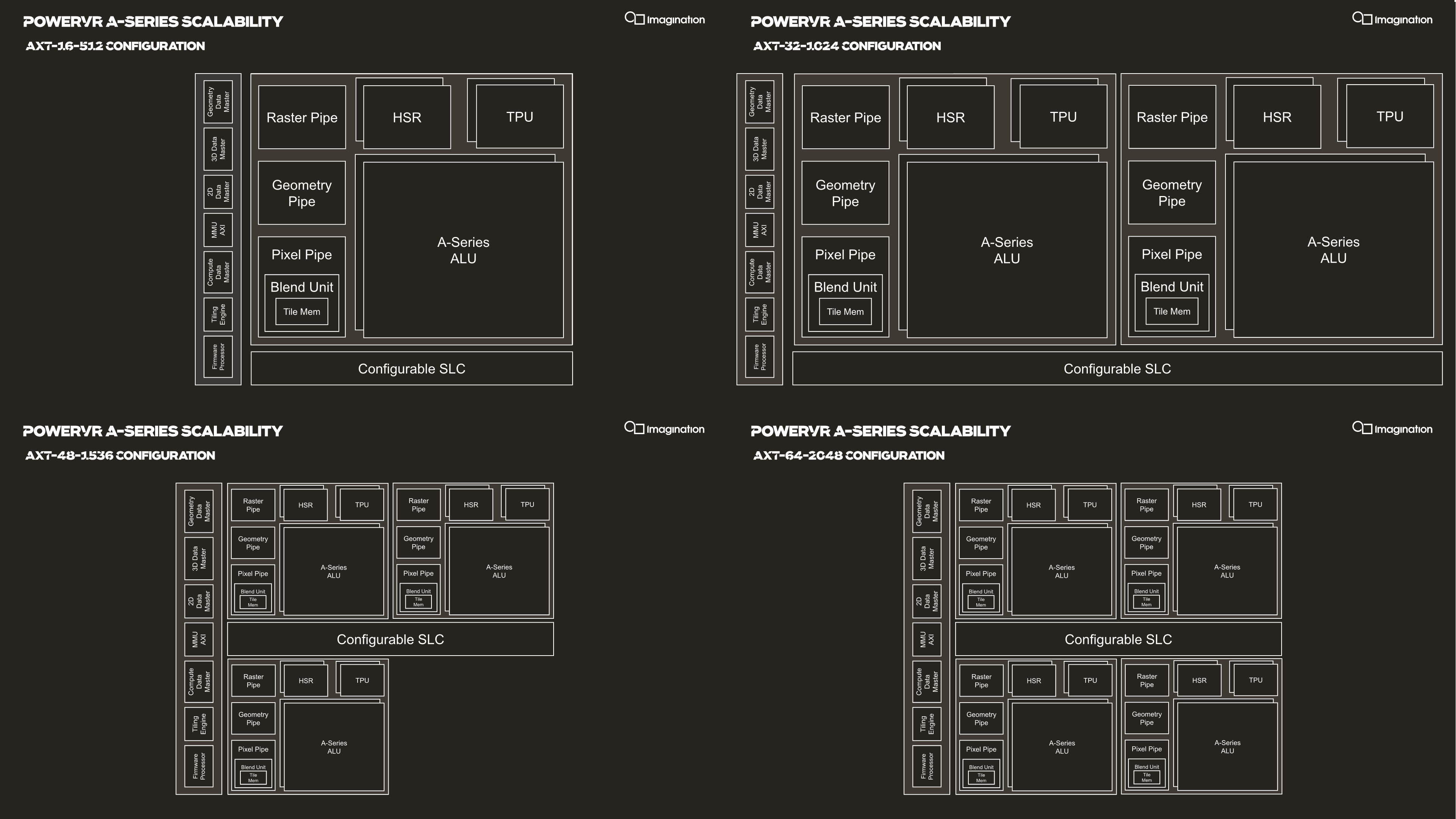
Scaling of SPUs across the AXT line happens in multiples of 16-512 across the range, both in terms of their product names as well as their texture and FLOPs/clock capabilities, which is rather simple to grasp and very quickly understand a configuration’s capabilities. As mentioned in the introduction, Imagination views the AXT-32-1024 as being the most popular choice for vendors targeting the high-end premium smartphone SoC segment, which possibly some vendors opting to go with the AXT-48-1536 for a larger area and lower clock speeds for more efficiency. The AXT-64-2048 would be a really big GPU which the company could build if there’s costumer interest.
| PowerVR GPU Comparison | ||||
| AXT-16-512 | GT9524 | GT8525 | GT7200 Plus | |
| Core Configuration |
1 SPU (Shader Processing Unit) - "GPU Core" 2 USCs (Unified Shading Clusters) - ALU Clusters |
|||
| FP32 FLOPS/Clock MADD = 2 FLOPs MUL = 1 FLOP |
512 (2x (128x MADD)) |
240 (2x (40x MADD+MUL)) |
192 (2x (32x MADD+MUL)) |
128 (2x (16x MADD+MADD)) |
| FP16 Ratio | 2:1 (Vec2) | |||
| Pixels / Clock | 8 | 4 | ||
| Texels / Clock | 16 | 8 | 4 | |
| Architecture | A-Series (Albiorix) |
Series-9XTP (Furian) |
Series-8XT (Furian) |
Series-7XT (Rogue) |
Comparing the smallest AXT-16-512 configuration with a single SPU and two USCs against similar configurations across the generations, we indeed see that the new A-Series does bring large architectural changes.
Imagination is marketing a 4x increase in ALU throughput, but again that’s against the 9XM GPUs, which are equal in ALU configuration to the Series-7XT in the table. However, it’s not to say that the increases aren’t any less impressive when comparing to the previous 9XTP family; a rise from 240 FLOPs/clock to 512 is still a 2.13x increase.
I think what’s actually more important to note here is the architecture has very big building blocks. At 512 FLOPs and 8 pixels per clock, an AXT SPU is significantly bigger than an Arm Mali-G77 core which comes in at “only” 64 FLOPs/clock and 2 pixels per clock, meaning an AXT core is roughly equivalent to eight G77 cores in computational power and four G77s in fillrate throughput, which is a massive difference in terms of design scaling. Naturally, in terms of effective density and power efficiency, few big cores will always win over a flock of small cores, as demonstrated by Qualcomm and Apple’s recent 2- and 4-core designs.
HyperLane Technology
Another new addition to the A-Series GPU is Imagination's “HyperLane” technology, which promises to vastly expand the flexibility of the architecture in terms of multi-tasking as well as security. Imagination GPUs have had virtualization abilities for some time now, and this had given them an advantage in focus areas such as automotive designs.
The new HyperLane technology is said to be an extension to virtualization, going beyond it in terms of separation of tasks executed by a single GPU.
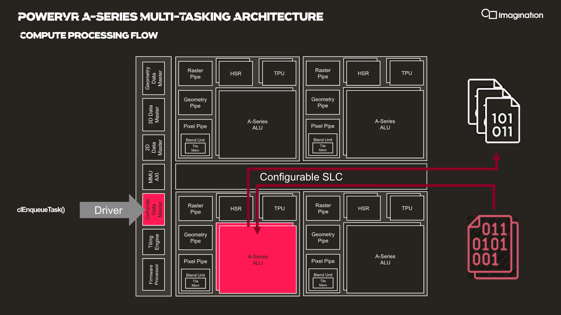
In your usual rendering flows, there are different kinds of “master” controllers each handling the dispatching of workloads to the GPU; geometry is handled by the geometry data master, pixel processing and shading by the 3D data master, 2D operations are handled by the 2D data, master, and compute workloads are processed by the, you guessed it, the compute data master.
In each of these processing flows various blocks of the GPU are active for a given task, while other blocks remain idle.
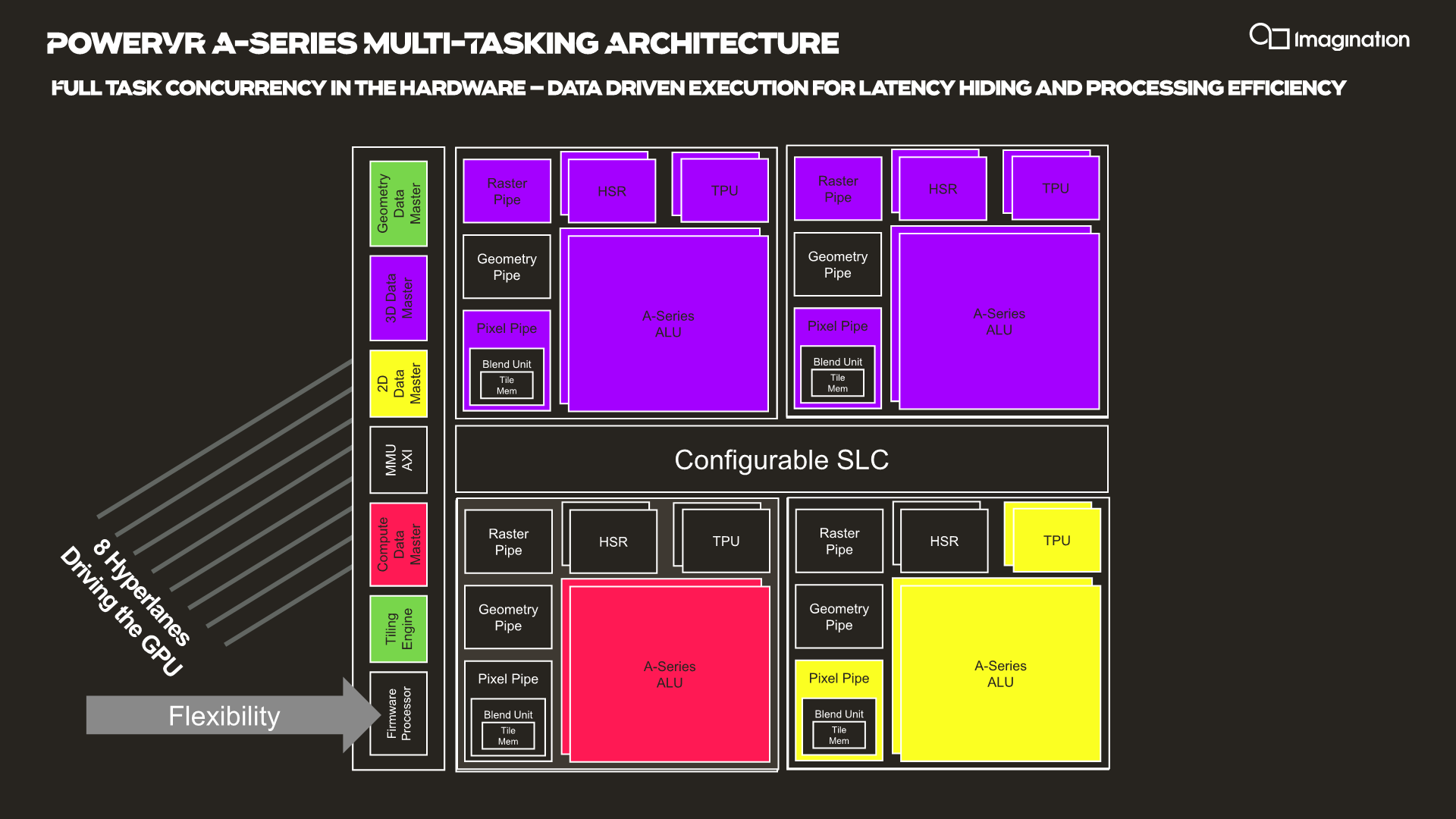
HyperLane technology is said to be able to enable full task concurrency of the GPU hardware, with multiple data masters being able to be active simultaneously, executing work dynamically across the GPU’s hardware resources. In essence, the whole GPU becomes multi-tasking capable, receiving different task submissions from up to 8 sources (hence 8 HyperLanes).
The new feature sounded to me like a hardware based scheduler for task submissions, although when I brought up this description the Imagination spokespeople were rather dismissive of the simplification, saying that HyperLanes go far deeper into the hardware architecture, with for example each HyperLane having being able to be configured with its own virtual memory space (or also sharing arbitrary memory spaces across hyperlanes).
Splitting GPU resources can happens on a block-level concurrently with other tasks, or also be shared in the time-domain with time-slices between HyperLanes. Priority can be given to HyperLanes, such as prioritizing graphics over a possible background AI task using the remaining free resources.
The security advantages of such a technology also seem advanced, with the company use-cases such as isolation for protected content and rights management.
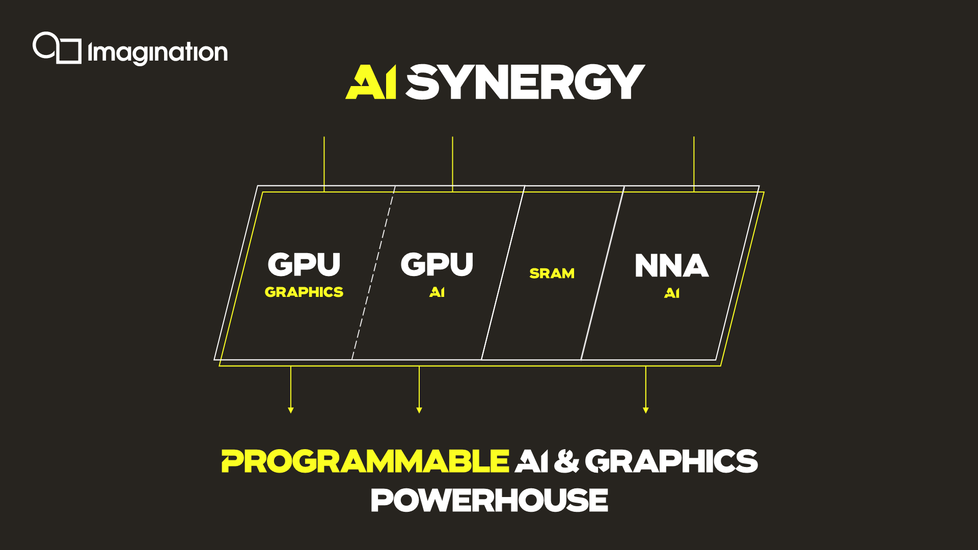
An interesting application of the technology is the synergy it allows between an A-Series GPU and the company’s in-house neural network accelerator IP. It would be able to share AI workloads between the two IP blocks, with the GPU for example handling the more programmable layers of a model while still taking advantage of the NNA’s efficiency for the fixed function fully connected layer processing.
Three Dozen Other Microarchitectural Improvements
The A-Series comes with other numerous microarchitectural advancements that are said to be advantageous to the GPU IP.

One such existing feature is the integration of a small dedicated CPU (which we understand to be RISC-V based) acting as a firmware processor, handling GPU management tasks that in other architectures might be still be handled by drivers on the host system CPU. The firmware processor approach is said to achieve more performant and efficient handling of various housekeeping tasks such as debugging, data logging, GPIO handling and even DVFS algorithms. In contrast as an example, DVFS for Arm Mali GPUs for example is still handled by the kernel GPU driver on the host CPUs.
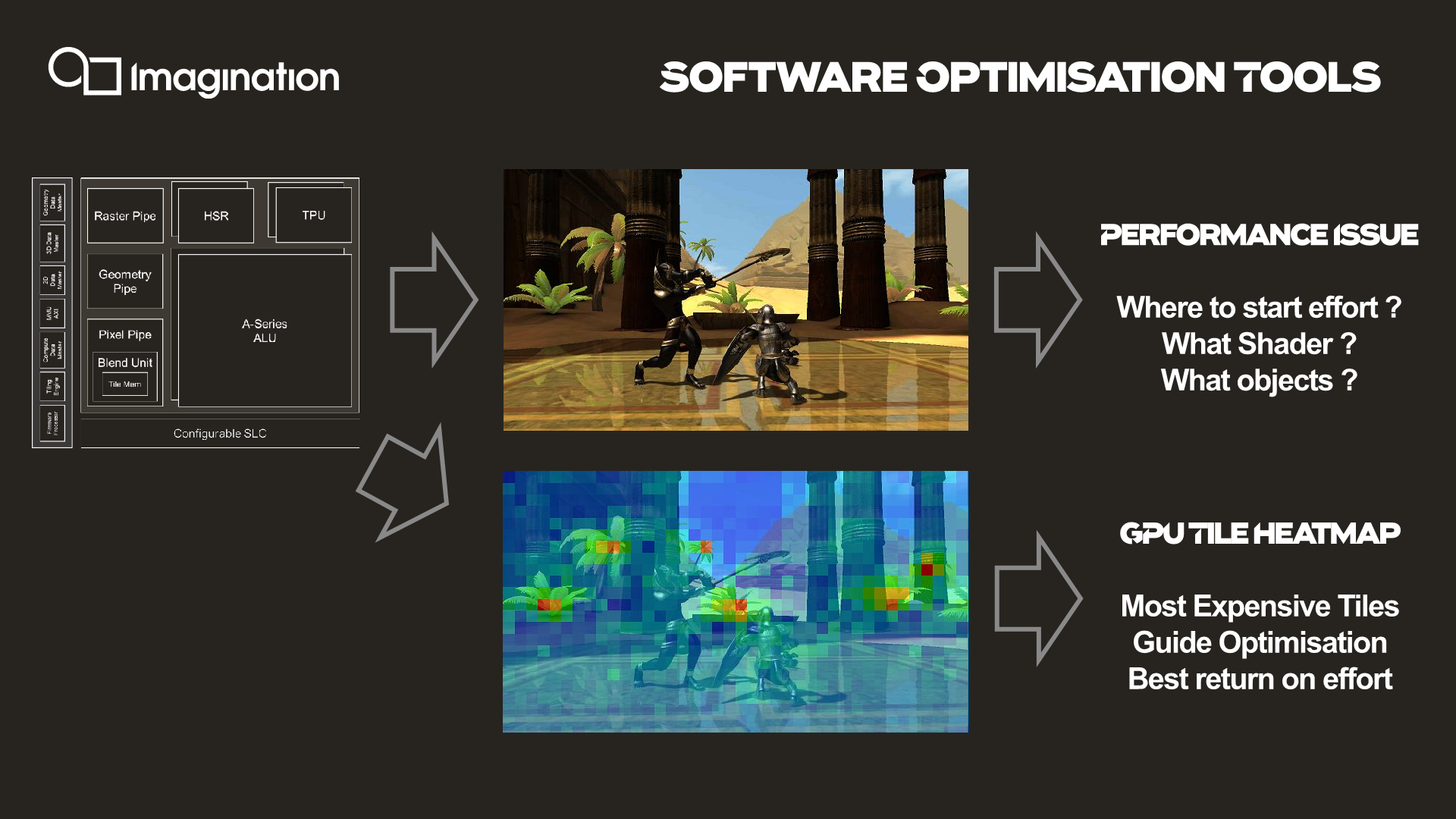
An interesting new development feature that is enabled by profiling the GPU’s hardware counters through the firmware processor is creating tile heatmaps of execution resources used. This seems relatively banal, but isn’t something that’s readily available for software developers and could be extremely useful in terms of quick debugging and optimizations of 3D workloads thanks to a more visual approach.
PPA Projections - Significant, If Delivered
Moving on, the A-Series improvements don’t mean much if we can’t put them into context in the competitive landscape.
As mentioned in the introduction, Imagination seem aware of the current PPA deficit that GPU vendor IP offers versus custom designs by more vertically integrated SoC vendors.
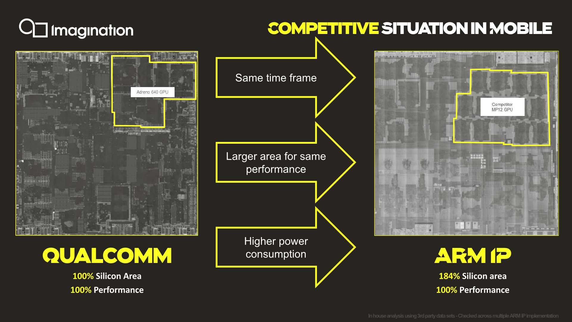
Starting off with a comparison between current generation Qualcomm GPU against an Arm GPU. Imagination didn’t specifically mention which designs we’re talking about here, but we do clearly see from the die shots that the SoCs being compared are the Snapdragon 855 and the Exynos 9820.
Here Imagination describes that for a similar performance level, Arm’s Mali GPUs are using ~184% the silicon area compared to Qualcomm’s Adreno implementation.
I do have some doubts about the validity of the comparison being made here, as these SoCs were not made on the same process node – Qualcomm's design is built on TSMC's denser 7nm process, while Samsung's Exynos uses their larger 8nm process. With that in mind, we take the metrics presented with a huge grain of salt as Imagination does say the figures are based on analysis of multiple Arm IP implementations rather than a single data-point.
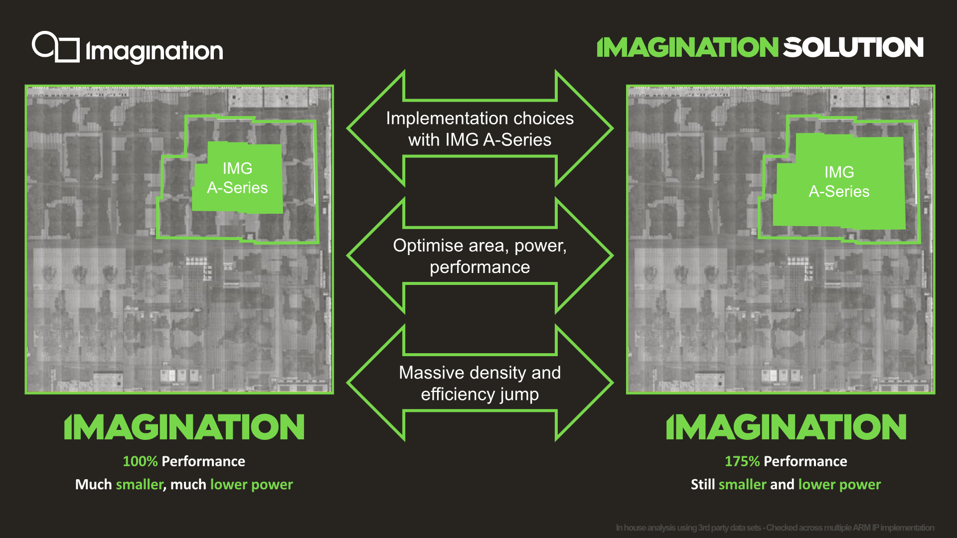
Projecting the A-Series against a current Mali-G76 implementation, targeting a performance level equivalent to current generation flagship implementations (~100fps in Manhattan 3.0), an A-Series GPU would achieve a significantly smaller GPU implementation requiring much less die area. The comparison implementation here would be an AXT-16-512 implementation running at slightly lower than nominal clock and voltage (in order to match the performance).
If a customer were to choose to use more die area to go wider and slower in clock (more efficient), while still maintaining an estimated area that would be smaller than a Mali GPU, it would roughly achieve a 75% performance advantage. The comparison here would be an AXT-32-1024 running quite far below nominal, giving it a large power efficiency advantage.
Of course, Imagination’s comparison here were made against the current generation Qualcomm and Arm GPUs, which aren't what it'll actually be competing against. Instead, by the time A-series SoCs ship, it will be competing against the next-generation Adreno as well as Mali-G77. We know Arm’s promised goals for the G77 and the improvements in performance per mm² and performance perf/W is around 1.2-1.4x, which we could generalize to 1.3x. Samsung’s upcoming Exynos 990 only promises a 20% performance increase, which is slightly below this projection. On the Qualcomm side and the upcoming Adreno generation, we’ll have to wait a few more days to be able to talk about details, but generally we expect improvements in the same ballpark.
Fortunately for Imagination, the projected PPA figures and advantages for the A-Series are high enough that they would still be notably ahead of both Qualcomm and Arm’s upcoming next generation GPUs, keeping a comfortable lead in either GPU area, or performance, depending on the configuration.
So far everything looks quite splendid – what remains to be seen if Imagination and their licensees are able to deliver on the projected figures.
Future Roadmap & Final Thoughts
The new A-Series architecture means to represent a reset for Imagination’s product offerings, representing a bright new future for the company. The new GPU IP is certainly impressive in terms of the PPA metrics that it promises to achieve, and if realized, it does have ramifications for the wider industry and the competitive landscape.
But even if the A-series can deliver on all of Imagination's promises, the company can't stop there. The competition is continuing to refine and improve their designs, and so must Imagination. To that end, along with today's announcement of the A-series, Imagination is also publishing a very broad roadmap for the next few years, outlining the upcoming GPU generations and their expected performance gains. All of this is especially important for SoC designers, who want to know what's coming down the pipe before making the effort to switch IP vendors.
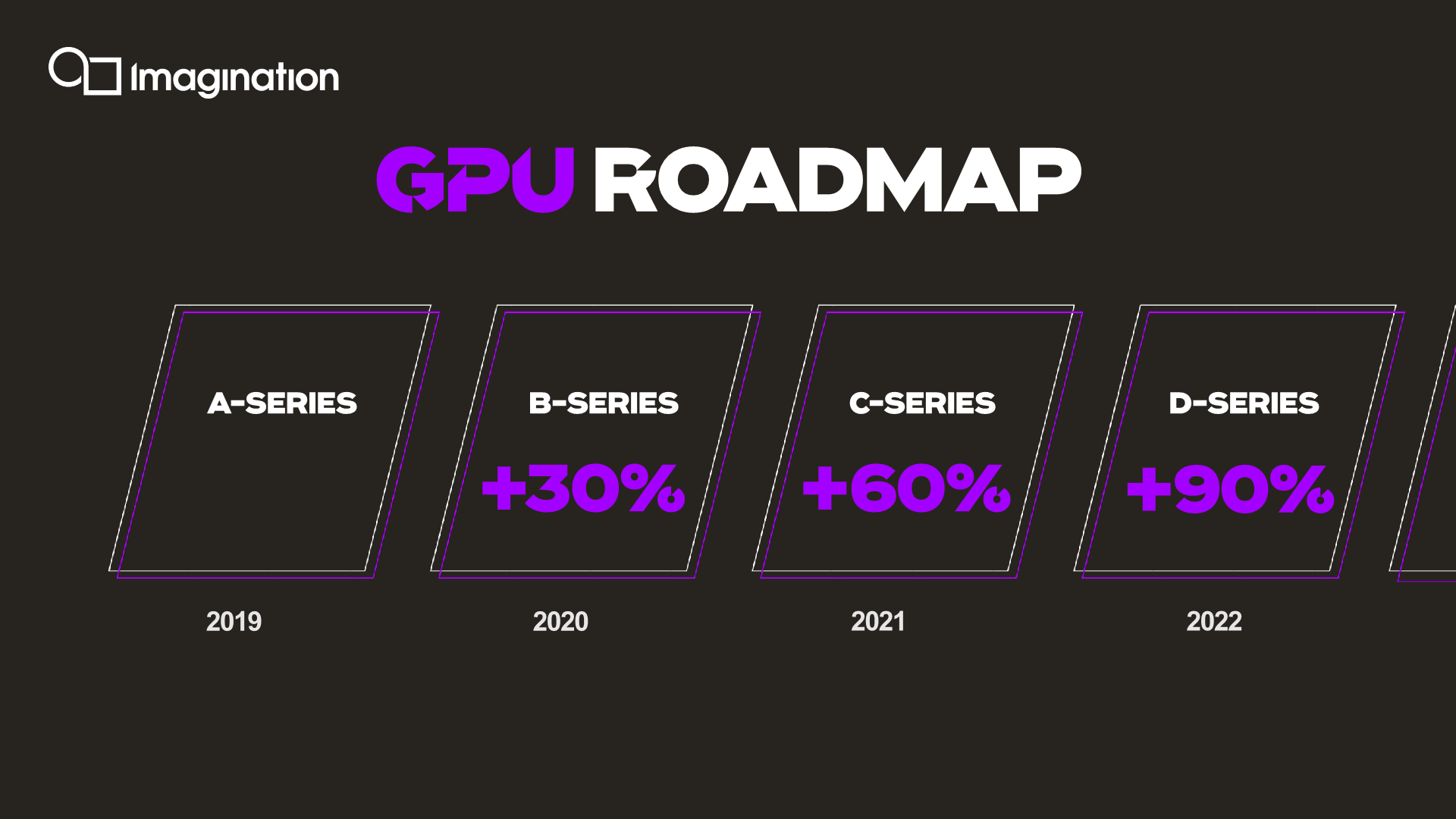
Imagination’s roadmap following the A-Series is seemingly very aggressive, promising yearly updates going forward, with large annual performance increases of 1.3x, or a 30% yearly compound annual growth rate. This is a much bigger goal than we’re used to historically, but it’s very much in line with the pace of progress we’ve seen from some vendors in the past, or even what Apple has managed to recently achieve over the last two generations.
For the A-Series, Imagination has adopted a public announcement schedule more similar to Arm’s, meaning that the A-Series has already been finished and licensed out to customers, with SoCs being designed and prepared to hit the market for 2020 – we’re assuming the latter part of 2020.
The B-Series is already well under way in terms of development and projected to be completed by next summer if the roadmap is to be taken as an accurate schedule, so at least Imagination has a strong path forward.
What’s important here for Imagination, is managing to actually achieve design wins for the new GPU IP in meaningful higher volume sockets. In terms of possible customers, it’s an increasingly small list, with most of them being the smaller Chinese SoC vendors such as RockChip, Unisoc (formerly Spreadtrum). Samsung is an unlikely client given their plans with AMD as well as custom GPU development, unless there happens to be some opportunity in the low and mid-range segments. HiSilicon likely is tied to Arm, if their plans of a custom GPU don’t pan out. This leaves MediaTek as one of the bigger clients, with the most opportunity and likelihood of adopting the A-Series. Holding onto more MediaTek SoC wins, instead of having them flip-flop between PowerVR and Mali, would be a big win for Imagination and its GPU group. With MediaTek now having re-entered the flagship SoC market, it seems like a very good match.
The wider semiconductor industry is said to be in an architecture revival phase, realizing the need for stronger designs in order to make up for decreasing yearly improvements in process performance. Imagination’s A-Series here seems to be a perfect example of such a revitalization, bringing with it massively impressive generational jumps. If the improvements pan out in practice, I do believe it could be a turning point for the company, and in the future we indeed might look back on it as being the most important launch in the company’s mobile history.


