Original Link: https://www.anandtech.com/show/6228/asrock-x79-extreme11-review-pcie-30-x16x16x16x16-and-lsi-8way-sassata
ASRock X79 Extreme11 Review: PCIe 3.0 x16/x16/x16/x16 and LSI 8-Way SAS/SATA
by Ian Cutress on September 3, 2012 10:15 AM EST- Posted in
- ASRock
- Motherboards
- X79
- LSI
- PLX
The end of summer marks the start of the X79 refresh line. We are, at best estimates, coming up to half-way in the Sandy Bridge-E life as the top of the line processor range before Ivy Bridge-E comes to market. Both chips will be expected to run on X79 and the next chipset. But in the meantime, manufacturers are coming up with ways to reinvigorate their X79 line up. So insert ASRock, and the ASRock X79 Extreme11. This motherboard comes with two PLX PEX 8747 chips, making up to 72 PCIe lanes available. This are split into 64 for the PCIe slots (x16/x16/x16/x16 capable), and eight are directed to an LSI SAS 2308 PCIe 3.0 chip, which allows RAID 0, 1 and 10 on eight SATA ports, for a peak throughput of up to 4.0 GBps from eight drives in RAID-0.
ASRock X79 Extreme11 Overview
In the ASRock X79 range, we have the Extreme3, the Extreme4, the Extreme4-M, the Extreme6, the Extreme7, the Extreme9, the Game Blaster equipped Extreme6/GB, two Fatal1ty motherboards and now the Extreme11. The ASRock X79 Extreme11 is designed to stretch both the X79 platform and your wallet – this motherboard will set you back a good $600 MSRP. For the hard cash, the motherboard has two main selling points.
Firstly, we have a pair of PLX PEX 8747 chips on board, both of which translate 16 of the CPU PCIe lanes into 32 for the PCIe slots each (for more information on how this works, please read our PLX PEX 8747 discussion). This gives the motherboard, as a whole, 72 PCIe 3.0 lanes to play with. The 64 lanes that come directly from the PLX chips go to the PCIe slots, to provide a peak x16/x16/x16/x16 mode with 4 GPU devices. However, the focus of this board is not in GPUs for gaming, but workstations with GPU accelerated features. In this arrangement, with all the PCIe slots populated, we get x16/x8/x8/x8/x8/x8/x8. If you believe the leaks/news online about an upcoming single slot GTX670, or want to purchase several single slot FirePro cards, then the ASRock will give you all that bandwidth as long as the user handles the heat.
The other eight lanes are taken direct from the CPU and put into an LSI SAS 2308 PCIe 3.0 chip. This chip supplies the board with eight SAS2 ports, which are also SATA 6 Gbps compatible. Through the chip, we have access to RAID 0, 1 and 10, (but no RAID 5 unfortunately), but due to the PCIe bandwidth, are not limited to the chipset like normal server chipsets like C602, C604 or C606. This results in our testing at a peak speed of 4.0 GBps with eight SSDs in RAID-0. However, the presumed real-world layout for this would be RAID-1 or RAID-10. It should be noted that there is also no cache associated with the LSI chip, and thus we only get speed increases above 64KB transfers.
The focus of the X79 Extreme11 is not the gamer. For gaming, ASRock have their Fatal1ty branding. ASRock want to aim at the workstation market, those that require PCIe functionality and an SAS enabled motherboard without having to go out and purchase a separate PCIe card. As a result, the ASRock X79 Extreme11 is also compatible with the 16xx, 26xx and some of the 46xx Xeons (link) from the launch BIOS, like the server compatible chipsets, and un-buffered ECC memory with those Xeons.
Other features onboard include dual Broadcom gigabit Ethernet ports which can be teamed, a Creative Sound Core3D audio solution, power delivery methodology through dual-stack MOSFETs and dual 8-pin CPU power connectors. As the X79 chipset does not have USB 3.0 as standard, ASRock have included Texas Instrument USB 3.0 controllers for a total of eight ports (4 on the back panel, 4 via two onboard headers) and a 2-port front USB panel included in the box. As expected with a board of this price we also get a full compliment of DIMM slots.
Performance on the X79 Extreme11 can be taken in different directions. It performs like most other X79 boards we have tested with the i7-3960X, although it does not have MultiCore Enhancement like the ASUS ROG motherboards. The throughput on the LSI chip scales well with drives, but the more drives you have the larger the transfer size has to be for scaling. Also with our ATTO testing, the chipset SATA ports tended to have better read speeds at lower transfer sizes. Power consumption is also an issue – having two PLX chips and an LSI chip adds a level of power draw depending on how the PCIe slots are populated. But as a motherboard aimed at workstation builds, power draw is not a primary feature here.
When deciding whether to recommend a motherboard such as the ASRock X79 Extreme11, we come across a dilemma. For workstation builders, money can potentially be no object. In terms of CPU performance, we would get the same here as we would do in the X79 Extreme4-M. The premium the user is paying for this product comes when PCIe bandwidth is the priority, but also wants a product that can handle SAS drives.
If you remember back to the ECS X79R-AX I reviewed back in January, this had SAS ports but they were not certified for SAS function. Gigabyte has released the X79S-UP5 which is based on the C606 chipset, so also comes with SAS ports but not any extra PCIe bandwidth. It is also worth nothing that on the C606 platforms that the ports are limited to SATA 3 Gbps and a peak of ~ 1.0 GBps (under Intel specifications). So for that the ASRock X79 Extreme11 is preferred.
Estimates for the PLX chip put the extra BOM cost of $40-$60 a piece, and the LSI chip cost is an unknown factor – perhaps $100+. But as of now this is the only consumer level board with the LSI 2308 controller equipped. So the premium must be paid. Purely as a workstation board I would happily recommend the ASRock X79 Extreme11. As a regular user or gamers board however, the cost could be a bit prohibitive compared to what else is available in the market.
Visual Inspection
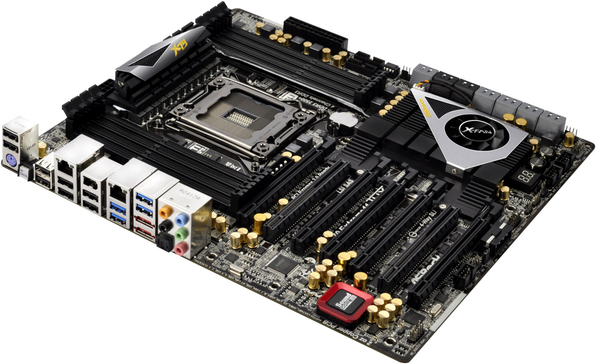
The X79 Extreme11, due to the extras on board, comes in at the loosely defined E-ATX form factor. In the case of the ASRock, this means an extra inch on the right hand side of the board. This also pushes the board away from the case mounting holes for more ports on the edge of the board, as noticed by the SATA ports below. The main feature that sticks out on first glance however is that all the PCIe slots are full length, and next to a rather large chipset heatsink (which also hides the two PLX chips and the LSI chip.
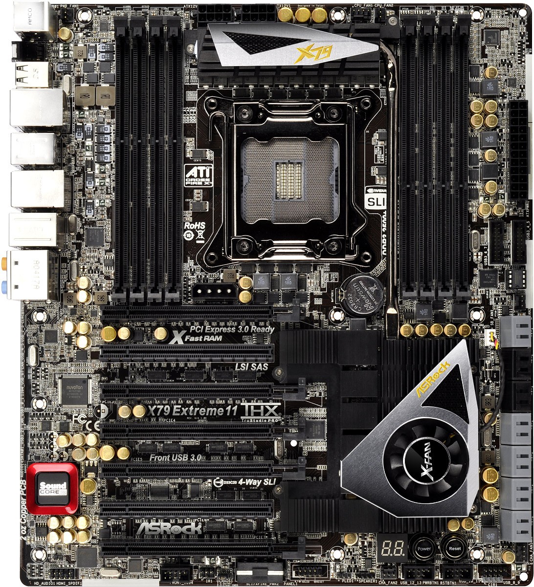
The socket area provides space for air coolers when only four RAM slots are populated. Given that this is aimed at the workstation crowd, it is more than likely that all the memory slots are occupied, thus an all-in-one liquid cooler is a good suggestion here. The board in total has six fan headers, four of which are reachable from the CPU socket – a 3-pin PWR header to the top left of the socket, two CPU headers (one 4-pin, one 3-pin) above the socket, and a 3-pin chassis header below the 24-pin ATX power connector and USB 3.0 headers. The other two are 4-pin and 3-pin chassis headers found at the bottom of the board.
The heatsink above the socket covers the power delivery for the motherboard, which ASRock state is a 24 phase (6x2x2 multiplexing) system. The heatsink is connected via a heatpipe to the flat chipset heatsink on the bottom of the board. The bottom heatsink is designed large and flat, with lots of fins and an additional fan to aid cooling. Our estimates are that this bottom heatsink has to deal with 35W+ (Chipset + PLX + PLX + LSI) dissipation, so the fan is a welcome to disperse the heat. However, our testing under dual GPU and above made this chipset fan run at a very high speed, which was definitely audible when idle as a high-pitched buzzing on the test bed. This could be mildly irritating, or not an issue when inside the case.
Along the right hand side of the board, we find the 24-pin ATX power connector, two USB 3.0 headers (powered by a Texas Instruments controller), a 3-pin fan header, and the SATA ports. ASRock have decided to use all the SATA ports from the chipset, and we also get eight from the LSI chip. So from top to bottom we have two SATA 6 Gbps in grey (chipset), four SATA 3 Gbps in black (chipset) and then we get the eight SAS2/SATA 6 Gbps ports in grey. All the ports on board are capable of RAID 0, 1 and 10, with the chipset ports also supporting RAID 5 via chipset specifications. Due to the routing we get some interesting results from this LSI SAS chip – all of which will be discussed in the review.
Along the bottom of the board we get our HD Audio header, a ClearCMOS header, a molex power connector (for PCIe), the front panel header, a 3-pin fan header, three USB 2.0 headers, a 4-pin fan header, a two-digit debug LED and power/reset buttons. The molex power connector is obviously the most interesting here, as typically in order to provide extra power ASRock put a molex connector above the PCIe slots. In this board they have used both, as with seven PCIe slots potentially drawing 535W (seven x 75W) this cannot all come through the ATX power connector. Personally, if ASRock had a choice between a top or bottom mounted molex connector, I would prefer the bottom such that cable management was easier.
The PCIe slots are simple to understand – each slot is designated either a primary slot (1,3,5,7) or a secondary slot (2,4,6). The primary slots are all x16 routed, via the PLX chips. The secondary slots are all x8 routed, and when occupied drop the speed of the primary slot underneath to x8 as well. Here is a crudely drawn chipset diagram to explain:
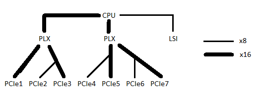
The forty lanes from the CPU are split into two lots of 16 for the PLX chips, and 8 lanes to the LSI chip. The PLX chips each take their 16 lanes (upstream) and produce 32 lanes each downstream. These 32 lanes are directed to into two sets of 16, each aimed at primary PCIe slots. The secondary slots that are linked to primary slots siphon off eight lanes (technically this is a point-to-point technology) when they are in use. This gives x16/-/x16/-/x16/-/x16 or x16/x8/x8/x8/x8/x8/x8.
Despite Sandy Bridge-E processors are not verified for PCIe 3.0 by specification, they do have the internals to do PCIe 3.0. These PLX chips are also PCIe 3.0, and thus in the BIOS PCIe 3.0 for all the slots can be enabled if required. In our testing, PCIe 3.0 did almost nothing for gaming – we saw minor increases of up to 0.5%-4% in Dirt3 compared to PCIe 2.0, and a 0.3% loss to 1.9% gain in Metro 2033. (Both games at 2560x1440 with all eye candy enabled using 7970s).
Also on board we get a Creative Core3D SoundBlaster chip for audio, which uses its own electromagnetic shielding to help improve audio signal transmission. Other products also specify if their motherboard uses a separate layer for audio – no such mention is provided by ASRock here.
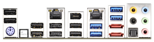
On the rear IO panel ASRock have equipped the X79 Extreme11 with a keyboard PS/2 port, eight USB 2.0 ports (black), a ClearCMOS button, dual gigabit Ethernet via Broadcom controllers, an IEEE1394 port, four USB 3.0 ports (TI controller), two eSATA ports, Optical SPDIF output and audio jacks. ASRock have potentially missed a trick here – the two USB 2.0 ports to the right of the ClearCMOS button could easily use a 4-bay USB 2.0 port hub, thereby removing one USB 2.0 header from the bottom of the board. Hopefully the additional routing would not be too difficult.
Board Features
| ASRock X79 Extreme11 | |
| Price | Link to Newegg |
| Size | ATX |
| CPU Interface | LGA2011 |
| Chipset | Intel X79 |
| Power Delivery | Intel Second Generation Core i7 Sandy Bridge E |
| Memory Slots |
Eight DDR3 DIMM slots supporting up to 64 GB Up to Quad Channel DDR3, 1066-2400 MHz ECC Memory with Xeon Processors |
| Onboard LAN | Dual Broadcom BCM57781 |
| Onboard Audio | Creative Sound Core3D |
| Expansion Slots |
1x PCIe 3.0 x16 3x PCIe 3.0 x16 (x8 when slots above are populated) 3x PCIe 3.0 x8 |
| Onboard SATA/RAID |
2x SATA 6 Gbps (Intel) 4x SATA 6 Gbps (Intel) 8x SAS2/SATA 6 Gbps (LSI SAS 2308) |
| USB |
14x USB 2.0 (8 rear panel, 6 onboard) 8x USB 3.0 (4 rear panel, 4 onboard) |
| Onboard |
2x SATA 6 Gbps 4x SATA 3 Gbps 8x SAS2/SATA 6 Gbps 2x USB 3.0 Headers (TI) 3x USB 2.0 Headers 6x Fan Headers 1x IEEE 1394 Header Power/Reset Switches Two-Digit Debug LED ClearCMOS Switch |
| Power Connectors |
1 x 24-pin ATX Power Connector 2x 8-pin CPU Power Connectors 2x 4-pin Molex Power Connectors |
| Fan Headers |
2 x CPU (one 4-pin, one 3-pin) 1 x PWR (4-pin) 3 x CHA (one 4-pin, two 3-pin) |
| IO Panel |
1x PS/2 Keyboard Port 1x Optical SPDIF Output 8x USB 2.0 Ports 4x USB 3.0 Ports (TI Controller) 2x eSATA 2x Broadcom GbE 1x IEEE1394 1x ClearCMOS Switch Audio Jacks |
| Warranty Period | 3 Years |
| Product Page | Link |
With a motherboard costing $600 MSRP, we should try and assign where that money is going. The two PLX chips and the LSI chip combined could be as much as $300 – asides from these additional extras, the dual NIC that can be teamed (combined with XFast LAN) is a good addition for a workstation board. The upgraded audio could be construed towards more audio based applications, thus some GPUs may help with encoding. As always, we like the fact of the Power/Reset buttons and two-digit LED for debugging.
ASRock X79 Extreme11 BIOS
As explained in our review of the ASRock Z77 Extreme9, the ASRock graphical BIOS system has gone through some minor evolutionary changes since the inception at the beginning of P67. On the X79 Extreme11 today, we see the next step in that evolution towards something a little more exciting to look at, as well as a reorganization of some menu options.
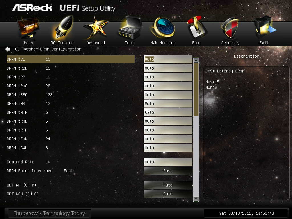
Regarding default settings, a couple of important points should be noted. The BIOS by default gives the PCI Express lanes as Gen 2.0, rather than a method of auto detection. Users of PCIe 3.0 graphics cards or PCIe devices should navigate to the North Bridge menu in order to set these lanes as Gen 3.0. The BIOS should come with audio cues to allow the user notifications as well. The final point is the memory – in our reviews of the X79 ROG range, those motherboards ran DDR3-2400 9-11-11 on our memory kit with a little bump in VTT and DRAM voltage. Unfortunately the ASRock X79 Extreme11 could not do this – we ended up running the system at DDR3-2133 9-11-11, which had little negative affect on our benchmark suite. It should also be noted that the current MultiCore Enhancement trend sweeping Z77 (and ASUS on X79) is not present here.
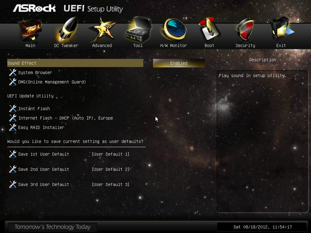
So the first thing to notice regarding the updated ASRock BIOS is the look – ASRock has added a space themed background, which provides better contrast than previous versions. The icons on the top row have also changed, along with the addition of a ‘Tool’ option, which moves some features (System Browser, OMG, BIOS Update, Profiles) into an easier-to-use menu.
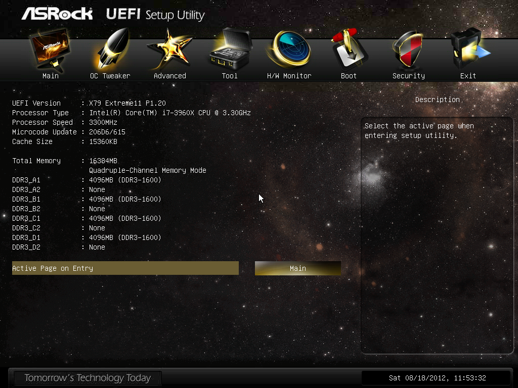
The main screen is slowly evolving into something we want as system builders and debuggers – we get the motherboard name, BIOS version, the CPU, the memory size and the current memory speeds. All we need now are temperature readings as well as voltage information to make the screen more complete. With the graphical BIOS scope at play, this information has the potential to be well presented. On the main screen is also an option to change the active page on entry – this will be handy for overclockers wanting to change options in the BIOS over successive reboots.
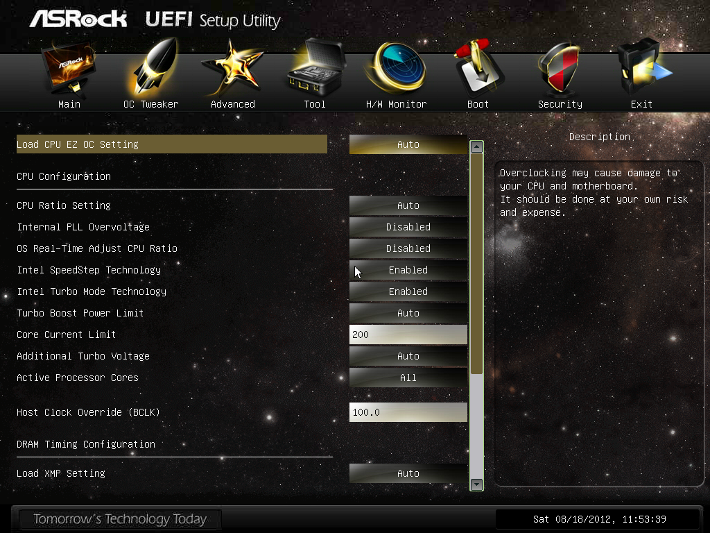
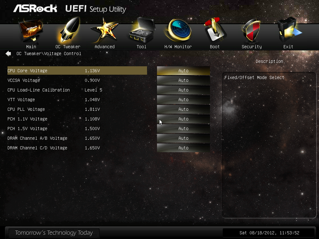
The overclocking action all happens in OC Tweaker, the next menu option on the top row. In OC Tweaker are the relevant CPU overclock settings – a series of automatic overclocks, manual choices with ratios, overvoltages, BCLK and Turbo Power Limits. For memory we also have the option to enable XMP or a memory strap, a further sub-menu is available to adjust individual sub-timings. CPU and memory voltages are dealt with in a separate menu at the bottom, along with load line calibration.

Overclocking on the X79 Extreme11 is discussed later in the review.
The ‘Advanced’ menu option houses various chipset configurations, such as the CPU and CPU Power Management (for enabling/disabling cores or power states), North Bridge configuration (for PCIe 2.0 or 3.0), South Bridge configuration (enabling/disabling onboard controllers), SATA configurations et al.
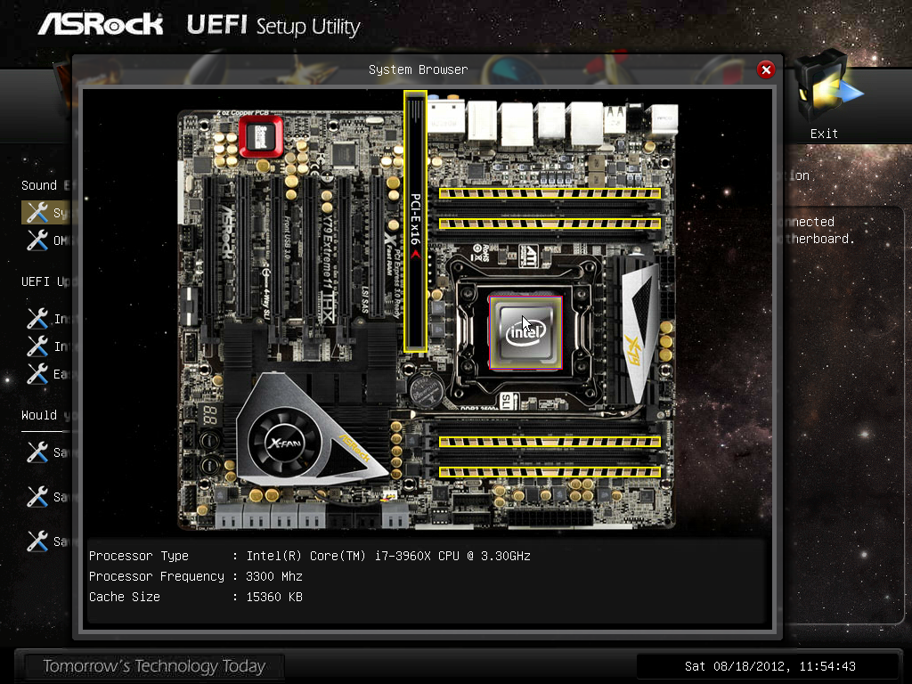
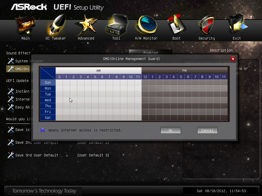
The new ‘Tool’ menu option leads us to all the newer features of ASRock BIOSes of late all under one heading. This means we get the System Browser, a top down look similar to Gigabyte’s 3D BIOS which lets us know if hardware has been recognized at the BIOS level, Online Management Guard (to enable/disable network ports based on system time), the ability to flash the BIOS, RAID installation, and profile saving. We have detailed these features in previous ASRock BIOS reports, but moving them under one menu makes a lot of sense.
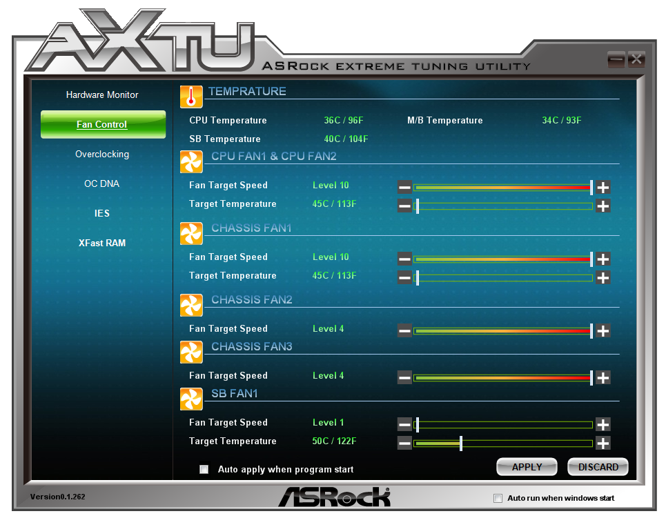
The H/W Monitor menu option shows the temperatures, fan speeds and voltages of the system. As I mention repeatedly, it would be worth having a few of these readings on the first screen of the BIOS, just to aid a little in debugging. Also in the H/W Monitor menu are our fan options.
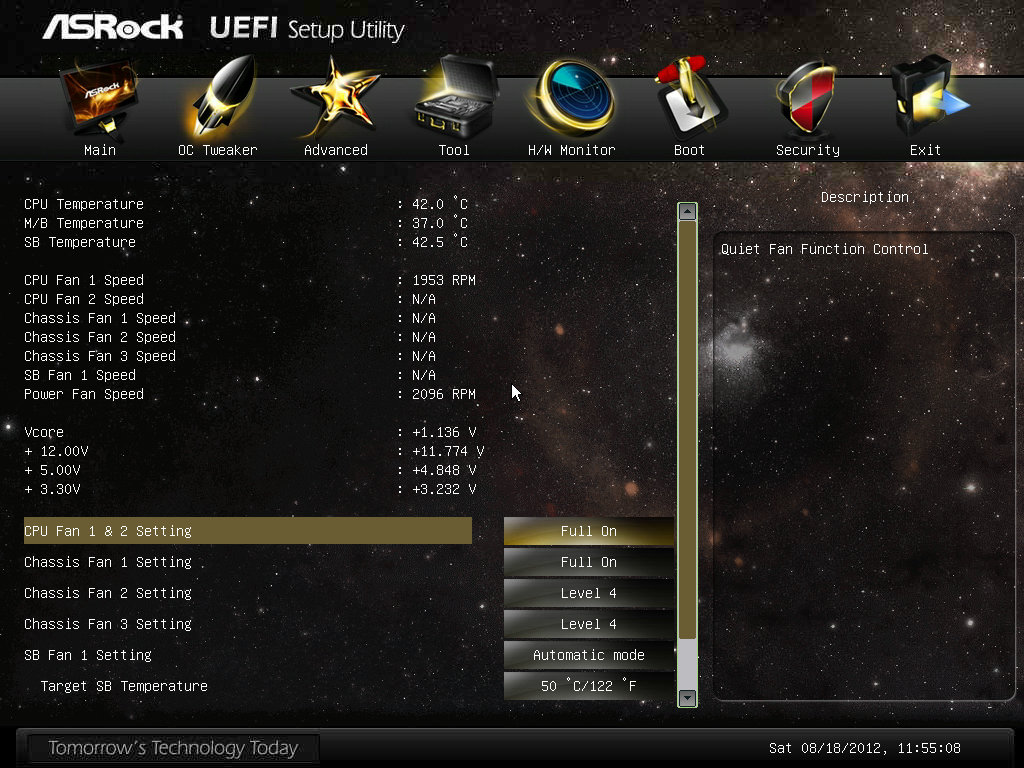
As with all ASRock boards of late, the main fan options allow for a target temperature and a ‘level’ in order to decide the slope of the ramp for fan speed against temperature. All other fans are given only a level to choose from for their ramp. There is plenty of scope to offer adaptive fan control if the motherboard manufacturers are willing to invest a little money and time into their fan controls – a lot is possible in software alone.


ASRock X79 Extreme11 Software
Despite the tweaks made to the presentation of the ASRock BIOS for the X79 Extreme11, we have not any tweaks to the standard software in the OS. The staple of the ASRock software package is the ‘555’ system, whereby ASRock state that their XFast RAM, XFast USB and XFast LAN can offer up to 5x performance (as long as the appropriate benchmark is chosen). Around this is the ASRock eXtreme Tuning Utility (AXTU), which houses the majority of the in-house made software for overclocking and fan controls.
The Driver CDs with ASRock products are always relatively easy to use – one click installs all the necessary drivers and another click to software with no intervention needed by the user.
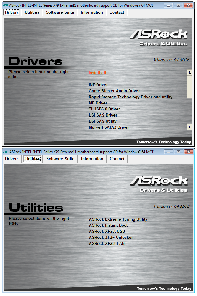
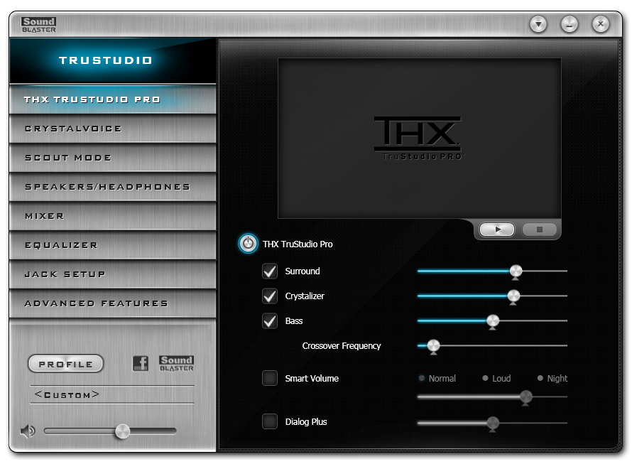
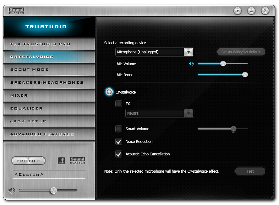
Also in the X79 Extreme11 package we get extra bundled software for the LSI chip called MegaRAID, and the Creative Sound Core3D chip on board also has its own software package in the form of TruStudio. Both will be detailed here.
AXTU (ASRock eXtreme Tuning Utility)
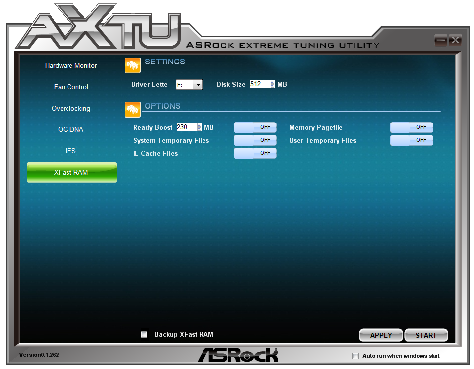
The AXTU utility attempts to be the centerpiece of the ASRock software, providing a hardware monitor, fan controls, overclocking controls, power saving utilities, and more recently, the inclusion of XFast RAM.
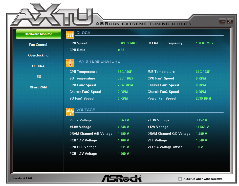
The hardware monitor is self describing, but the fan controls echo the ones scene on many ASRock boards of past. Instead of a simple graph demonstrating RPM % as a function of temperature, ASRock give us the option to choose a target temperature, then a ramp in the form of a level 1-10 option. One assumes that Level 10 is the most aggressive, but it is unknown if that ramp is the sharpest or the shallowest – it is hard to define aggressive in this context. Other fan headers are also given ramp options without the target temperature. It would be relatively very easy to knock up some software to actually control these fans properly relating to the temperature sensors on board – a focused effort is required by the manufacturer in order to envisage such controls though.
The overclocking tools offer BCLK and CPU ratio adjustments, as well as voltages. It strikes me as odd that the CPU voltage is offered as an offset, but the memory voltage is offered as a fixed value. This could be because of how these voltages are determined electrically, and the fact that this software has to be able to deal with many processors that all have different VIDs, but that should not deter the software from providing both an actual and an offset option.

The XFast RAM bit of the software is what we find most interesting. Due to the X79 platform, we have functionality up to 64 GB of memory. The ideal scenario would be to partition some of this off into a RAM Disk or a RAM Cache – this is exactly what XFast RAM does. We can allocate a disk size, and then ask the software to configure this RAM Disk as storage for temporary or cache files in order to speed up processing.
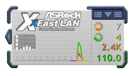
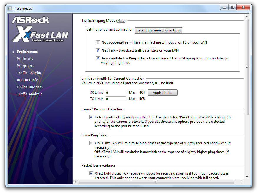
XFast LAN
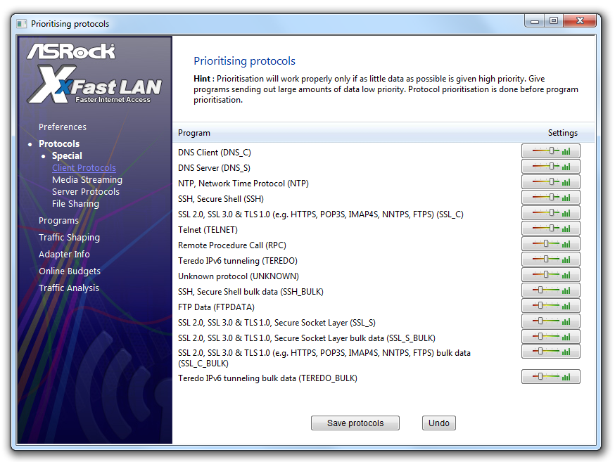
The XFast LAN software is ASRock’s re-branding of cFosSpeed, a software management tool for networking capabilities. The retail price of around 10 euros is absorbed by ASRock, presumably with some bulk sales deal, and for a little extra CPU power used, the network traffic can be monitored and shaped as required for all networking devices.
XFast USB
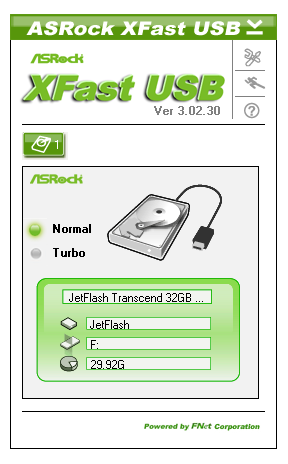
The XFast USB software is a staple part of the ASRock package. This is licensed software with ASRock re-branding works on the principle that the default drivers for USB ports in Windows 7 are flawed. By invoking a rewritten driver when a device is inserted, the USB port can call upon BOT (Bulk Only Transfer) commands in order to improve throughput (at the expense of latency). In our testing this driver increases speed for large transfer size files by a good margin, although for smaller transfers the UASP commands offered by other manufacturers offer an advantage.
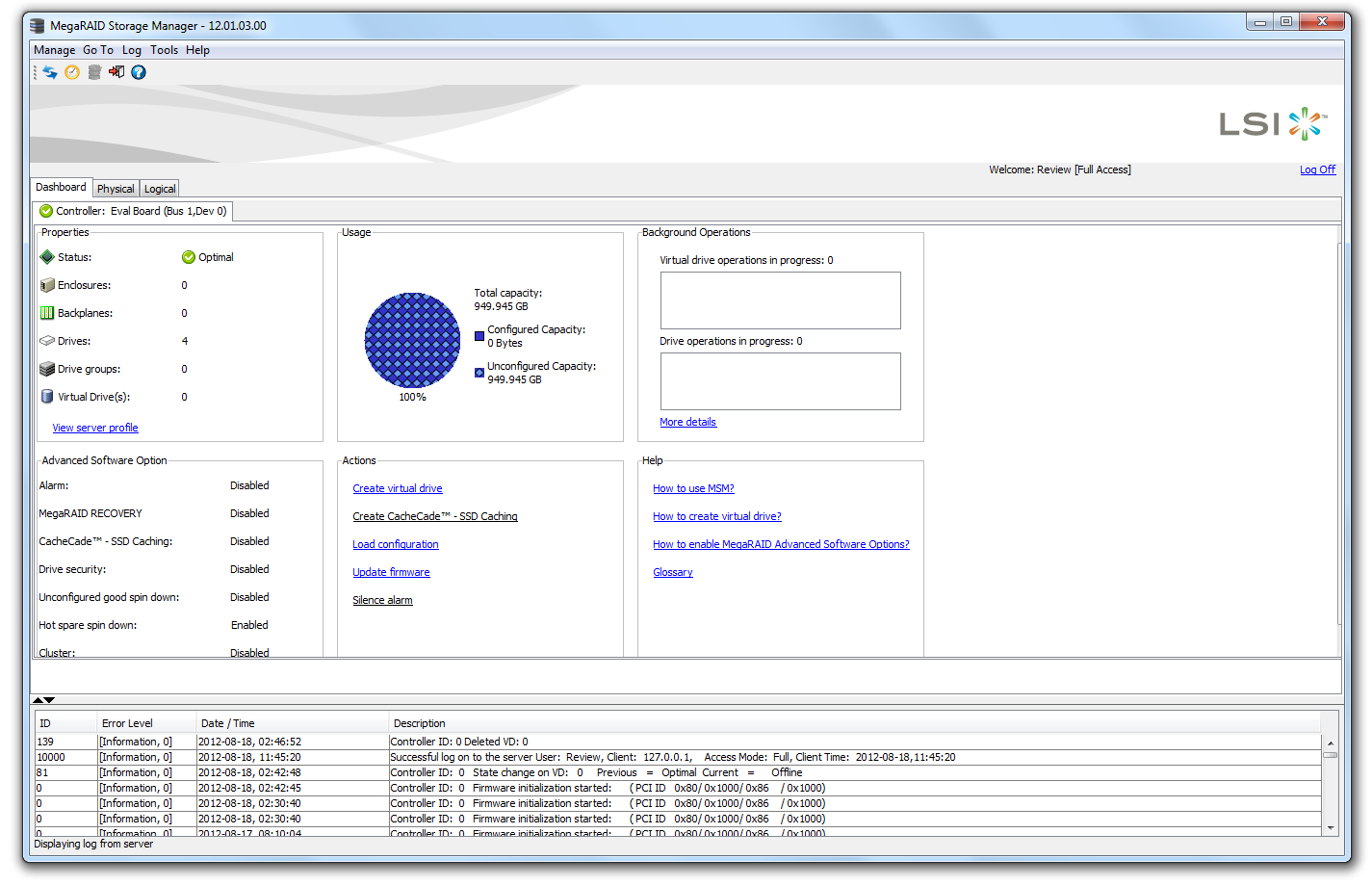
MegaRAID
The MegaRAID software comes direct from LSI, and is used to manage the SAS ports on the motherboard. The main feature of the software is to create and manage the RAID arrays – either RAID 0, 1 or 10. In our testing later, we will show the functionality when we test all eight ports at RAID-0, however due to the software we were limited to a 64 KB stripe size in our arrays.
The MegaRAID software allows users to define an array in a ‘Simple’ or ‘Advanced’ mode.

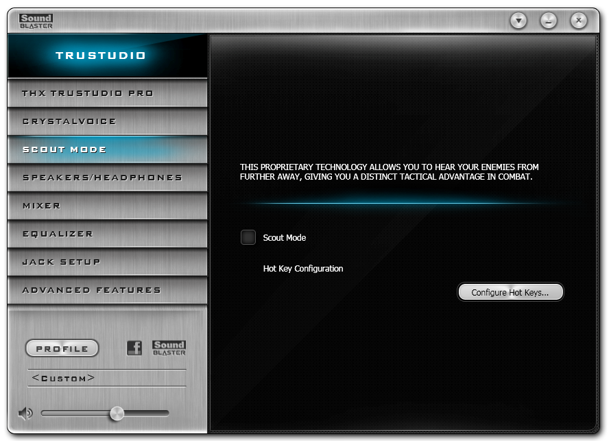
TruStudio
The audio software comes direct from Creative, and offers a wide range of manipulation techniques for your audio, including a proprietary technology called scout mode, which we assume is a software filter to increase the volume of typical footstep frequency sounds. The software also allows for a mixer, and equalizer, jack setups and voice filters for VOIP.


ASRock X79 Extreme11 In The Box
For the price tag, we expect a lot of extras in the box for what is ASRock’s high end model. Previously we have seen additional Front USB panels and/or WiFi connectors available in ASRock’s packages. With the X79 Extreme11, we get the following:
Rear IO Panel
Manual
Driver DVD
Six SATA cables
Two SATA to Molex Connectors
Two Short SLI Fingers
One Long SLI Finger
One Rigid 3-Way SLI Finger
Front USB 3.0 Panel
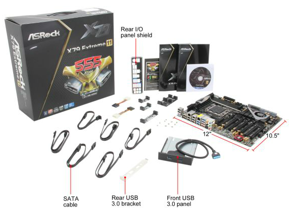
Personally, with the inclusion of the PLX and the LSI chips, I would have expected either a full compliment of SATA cables or a four-way SLI connector. There would have also been scope to increase the Front USB panels to either two, or a larger 5 1/4" bay with four ports and two connectors (depending on if workstation type cases came with USB 3.0). With boards like this, it might be worthwhile motherboard companies allying with a case manufacturer as a suggested build scenario.
Voltage Readings
After my first publication of OCCT voltage readings, a few readers responded with a more in-depth reasoning behind some of the results we were seeing. With this in mind, I would like to re-describe what we are doing with this test, and how it comes about.
Much of what an enthusiast overclocker does is monitor CPU temperature and voltage. Whatever settings a user places in the BIOS or OS is at the mercy of the motherboard - in terms of actually setting the values and reporting the values back. As an enthusiast, we have to rely on what readings we get back, and hope that motherboard manufacturers are being honest with their readings.
Take CPU voltage. What we as a user see in CPU-Z or OCCT is a time-averaged value that hides voltage ripple (if any) for power delivery. It is very easy for a motherboard manufacturer to hide this value, or to disregard slight deviations and report a constant value to the user. The CPU voltage reading can be taken at a variety of places on the power plane, which can vary between motherboards and manufacturers, meaning that each reading is essentially not comparable with the other. Nevertheless, as an enthusiast, we will constantly compare value A with value B.
Whether or not I can achieve 4.7 GHz with 1.175 volts on a particular board is inconsequential - your motherboard may perhaps produce the same result with a reading at 1.200 volts. The only way to test the actual value is with consistent methodology is via an oscilloscope connected to similar points on each board. This may sound like taking an OCCT reading is therefore redundant.
However, motherboards have settings relating to load line calibration. As load is applied to the CPU, the voltage across the processor decreases (VDroop). Load Line calibration essentially attempts to control this level of droop, by increasing voltage when voltage drops are detected away from a fixed value. Manufacturers have different ideas on how to modify LLC with respect to load, or whether the level of modification should be controlled by the user. Some manufacturers offer the option at a variety of levels, such that overclockers can be sure of the applied setting (even if it increases peak voltage, as explained by AnandTech in 2007).
By doing a full load OCCT test, we are essentially determining both how aggressive the motherboard is reporting the CPU voltage under load and how aggressive load line calibration is performing (from the point of view of the user without an oscilloscope or DVM). If someone has one of the motherboards we have tested and you have a different one, variations in load voltage should describe the offset you may require for overclock comparisons.
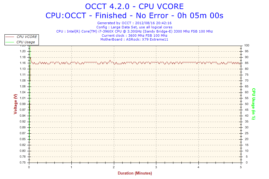
Like most ASRock boards, we see a small variation in the voltage reading under OCCT. Note that as OCCT is itself a time-smoothed reading of the ripple, perhaps the ASRock solution is not be as smooth as it could be. Nevertheless, I had no voltage issues on the board itself, and the X79 Extreme11 does a good job keeping around the 1.160 volt region during load at stock settings.
ASRock X79 Extreme11 Overclocking
Experience with ASRock X79 Extreme11
Overclocking with this board has mirrored a lot of the overclocking experiences of ASRock boards of late. The automatic overclock settings are often stable with just a smidge of extra voltage to ensure stability, while manual overclocking can suffer from overheating VRMs causing declocks. We get a similar scenario here.
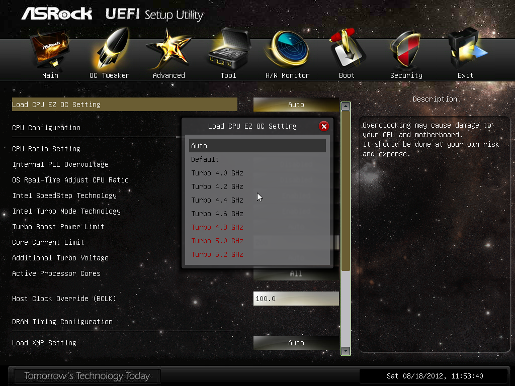
Manual overclock options are all in the BIOS – unlike Z77 options, we only get the ‘CPU EZ OC’ option here which offers 4.0 GHz to 5.2 GHz on our i7-3960X processor in 200 MHz steps. Each option provides a CPU voltage and Load Line Calibration appropriately, with a failed overclock either BSOD at boot or not even passing POST, requiring a ClearCMOS.
Overclock options are all essentially in the BIOS as well – the options via software are limited at best. In the BIOS we are free to change the CPU ratio and multiplier in the main OC Tweaker menu, but voltages, LLC and memory are in other menus. Each is easily navigable from the main OC Tweaker menu.
Methodology:
Our standard overclocking methodology is as follows. We select the automatic overclock options and test for stability with PovRay and OCCT to simulate high-end workloads. These stability tests aim to catch any immediate causes for memory or CPU errors.
For manual overclocks, based on the information gathered from previous testing, starts off at a nominal voltage and CPU multiplier, and the multiplier is increased until the stability tests are failed. The CPU voltage is increased gradually until the stability tests are passed, and the process repeated until the motherboard reduces the multiplier automatically (due to safety protocol) or the CPU temperature reaches a stupidly high level (100ºC+).
Our test bed is not in a case, which should push overclocks higher with fresher (cooler) air. We also are using Intel's All-in-one Liquid Cooler with its stock fan. This is a 120mm radiator liquid cooler, designed to mimic a medium-to-high end air cooler.
Automatic Overclock:
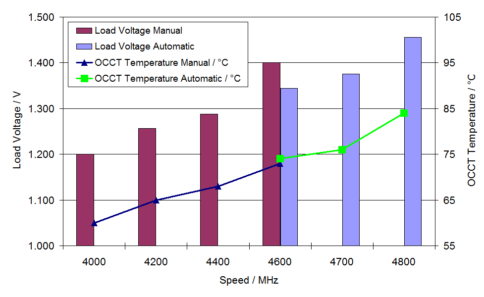
With the CPU EZ OC setting options, each of them were selected one by one, then booted and stress tested. Here are our results:
At the 4.0 GHz setting, the BIOS set the CPU LLC to Level 5 (low) and VCore on Auto. This led to a load voltage in the OS of 1.200 volts, with peak temperatures reaching 59°C during PovRay and 60°C during OCCT.
At the 4.2 GHz setting, the BIOS set the CPU LLC to Level 5 (low) and the VCore to a +0.040 volt offset. This led to a load voltage in the OS of 1.256 volts, with peak temperatures reaching 62°C during PovRay and 65°C during OCCT.
At the 4.4 GHz setting, the BIOS set the CPU LLC to Level 5 (low) and the VCore to a +0.080 volt offset. This led to a load voltage in the OS of 1.288 volts, with peak temperatures reaching 67°C during PovRay and 68°C during OCCT.
At the 4.6 GHZ setting, the BIOS set the CPU LLC to Level 3 (medium) and the VCore to a +0.130 volt offset, as well as enabling PLL Overvoltage. This led to a load voltage in the OS of 1.400 volts, with peak temperatures reaching 79°C during PovRay and 73°C during OCCT.
At the 4.8 GHz setting, the BIOS set the CPU LLC to Level 1 (high) and the VCore to a fixed 1.440 volt offset, as well as enabling PLL Overvoltage. This setting was not stable, resulting in a BSOD during boot.
At the 5.0 GHz setting, the BIOS set the CPU LLC to Level 1 (high) and the VCore to a fixed 1.460 volt offset, as well as enabling PLL Overvoltage. This setting was not stable, resulting in the board failing to POST.
At the 5.2 GHz setting, the BIOS set the CPU LLC to Level 1 (high) and the VCore to a fixed 1.500 volt offset, as well as enabling PLL Overvoltage. This setting was not stable, resulting in the board failing to POST.
Manual Overclock:
For our manual overclock testing, we start with PLL Overvoltage enabled by default (as required by Sandy Bridge over a certain OC) as well as Load Line Calibration set to Level 1 (high) to ensure stable voltages. We start with the CPU multiplier at 46x and a BIOS voltage of 1.350 volts. Here are our results.
At 46x, the BIOS setting of 1.350 volts was stable, giving 1.344 volts in the OS at load. This gave peak temperatures of 71°C during PovRay and 74°C during OCCT.
At 47x, the minimum stable voltage came from a BIOS setting of 1.375 volts, giving 1.376 volts in the OS at load. This gave peak temperatures of 76°C during PovRay and OCCT.
At 48x, the minimum voltage stable came from a BIOS setting of 1.450 volts, giving 1.456 volts in the OS at load. This gave peak temperatures of 84°C during PovRay and OCCT.
Beyond this speed, the system kept throttling down to 46x during load. Even when options were changed in the BIOS – CPU Thermal Throttling was off and Power Limits were raised, the system still reduced the clock speed at load.
Many thanks to...
We must thank the following companies for kindly donating hardware for our test bed:
OCZ for donating the Power Supply and USB testing SSD
Micron for donating our SATA testing SSD
G.Skill for donating our memory kits
ASUS for donating AMD GPUs and some IO Testing kit
ECS for donating NVIDIA GPUs
ASRock and ADATA for organizing loan of the RAID SSDs
Test Setup
| Processor | Intel i7-3960X (6C/12T, 3.3 GHz) |
| Motherboards | ASRock X79 Extreme11 |
| Cooling | Intel All-In-One Liquid Cooler |
| Power Supply | OCZ 1250W Gold ZX Series |
| Memory | GSkill RipjawsZ 4x4 GB DDR3-2400 9-11-11 Kit 1.65 V |
| Memory Settings | XMP |
| Video Cards |
ASUS 7970 3GB GDDR5 ECS GTX 580 1536MB |
| Video Drivers |
Catalyst 12.3 NVIDIA Drivers 296.10 |
| Hard Drive |
Corsair Force GT 60GB Micron RealSSD C300 256GB |
| Case | Open Test Bed - CoolerMaster Lab V1.0 |
| Operating System | Windows 7 64-bit |
| SATA Testing | Micron RealSSD C300 256GB |
| RAID Testing | ADATA SX910 256GB |
| USB 2/3 Testing | OCZ Vertex3 240GB |
Power Consumption
Power consumption was tested on the system as a whole with a wall meter connected to the OCZ 1250W power supply, while in a dual 7970 GPU configuration. This power supply is Gold rated, and as I am in the UK on a 230-240 V supply, leads to ~75% efficiency > 50W, and 90%+ efficiency at 250W, which is suitable for both idle and multi-GPU loading. This method of power reading allows us to compare the power management of the UEFI and the board to supply components with power under load, and includes typical PSU losses due to efficiency. These are the real world values that consumers may expect from a typical system (minus the monitor) using this motherboard.
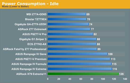
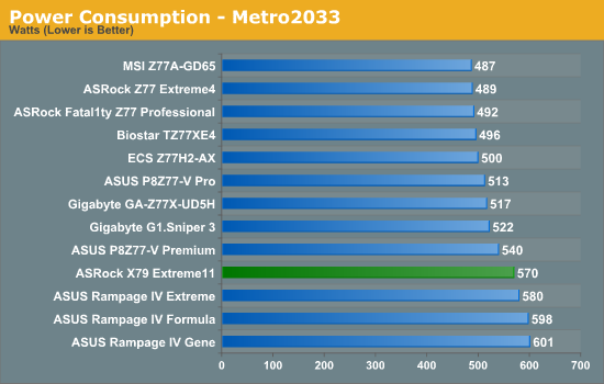
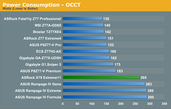
Despite the fact that the PLX chips can be power gated when not in use, at idle there is still a little overhead in power usage from the PLX+LSI combination. Nevertheless, the additional power required by the ASUS ROG boards at loading means that the ASRock draws less power during both Metro 2033 and OCCT.
POST Time
Different motherboards have different POST sequences before an operating system is initialized. A lot of this is dependent on the board itself, and POST boot time is determined by the controllers on board (and the sequence of how those extras are organized). As part of our testing, we are now going to look at the POST Boot Time - this is the time from pressing the ON button on the computer to when Windows starts loading. (We discount Windows loading as it is highly variable given Windows specific features.) These results are subject to human error, so please allow +/- 1 second in these results.
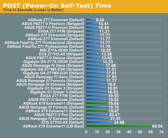
Unlike other ASRock motherboards, the X79 Extreme11 actually has a long time to boot. Even longer if you decide to boot from the LSI chip, or have Intel RAID arrays present.
USB Speed
For this benchmark, we run CrystalDiskMark to determine the ideal sequential read and write speeds for the USB port using our 240 GB OCZ Vertex3 SSD with a SATA 6 Gbps to USB 3.0 converter. Then we transfer a set size of files from the SSD to the USB drive using DiskBench, which monitors the time taken to transfer. The files transferred are a 1.52 GB set of 2867 files across 320 folders – 95% of these files are small typical website files, and the rest (90% of the size) are the videos used in the Sorenson Squeeze test.
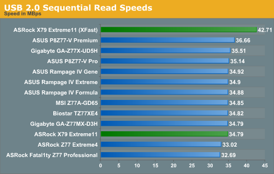
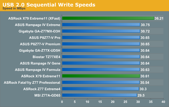
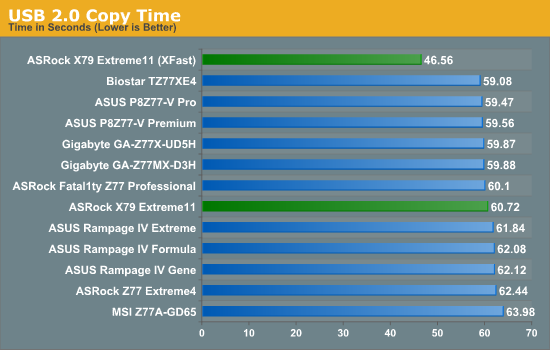
Nothing odd comes out of any USB 2.0 testing.
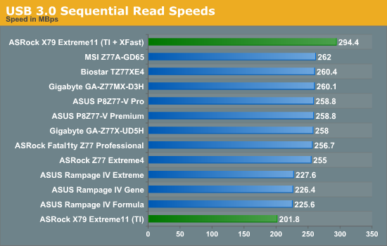
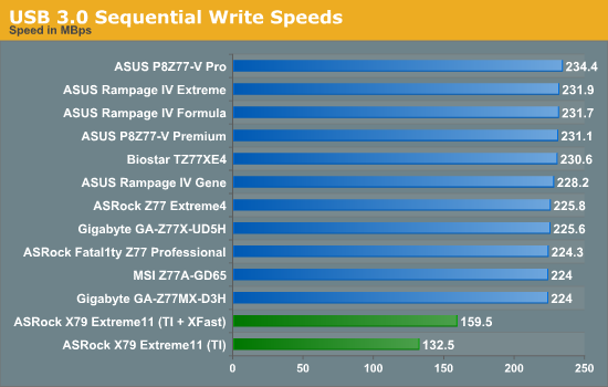
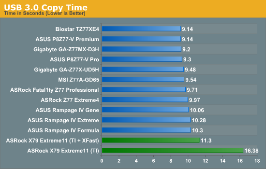
While the Z77 chipset has USB 3.0 native to the chipset, the X79 motherboards have controllers. In the case of the ASRock X79 Extreme11, we have Texas Instruments based USB 3.0 controllers, which perform rather badly in USB 3.0 writes compared to those found on the ASUS ROG boards.
SATA Testing
We also use CrystalDiskMark for SATA port testing on a C300 drive. The sequential test (incompressible data) is run at the 5 x 1000 MB level. This test probes the efficiency of the data delivery system between the chipset and the drive, or in the case of additional SATA ports provided by a third party controller, the efficiency between the controller, the chipset and the drive.
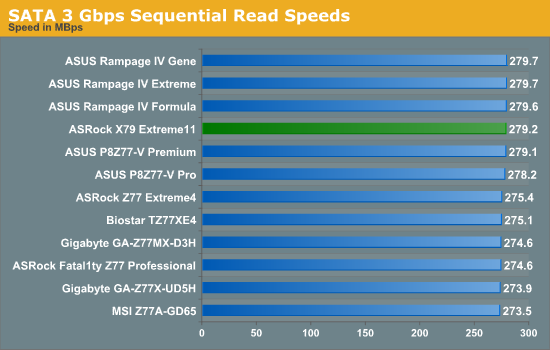
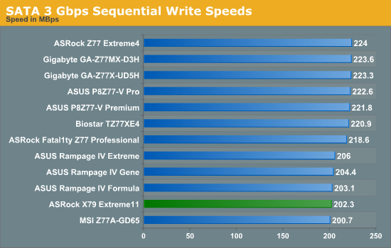
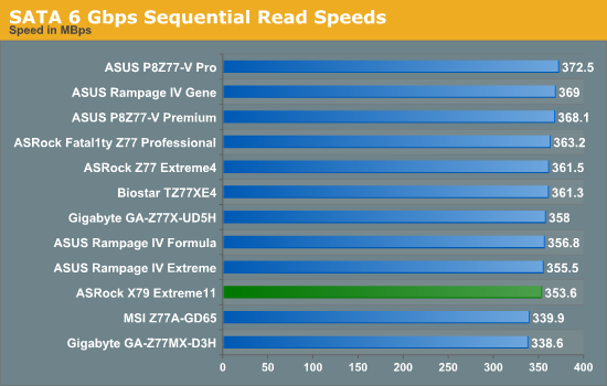
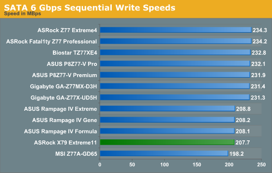
Nothing out of the ordinary comes out of our SATA testing - the SATA writing speed is split when comparing the X79 and Z77 platforms. Testing on the LSI ports will be in a later page of this review.
DPC Latency
Deferred Procedure Call latency is a way in which Windows handles interrupt servicing. In order to wait for a processor to acknowledge the request, the system will queue all interrupt requests by priority. Critical interrupts will be handled as soon as possible, whereas lesser priority requests, such as audio, will be further down the line. So if the audio device requires data, it will have to wait until the request is processed before the buffer is filled. If the device drivers of higher priority components in a system are poorly implemented, this can cause delays in request scheduling and process time, resulting in an empty audio buffer – this leads to characteristic audible pauses, pops and clicks. Having a bigger buffer and correctly implemented system drivers obviously helps in this regard. The DPC latency checker measures how much time is processing DPCs from driver invocation – the lower the value will result in better audio transfer at smaller buffer sizes. Results are measured in microseconds and taken as the peak latency while cycling through a series of short HD videos - under 500 microseconds usually gets the green light, but the lower the better.
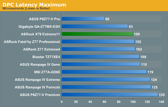
ASRock have a good standing in our DPC testing, and the X79 Extreme11 is no different. It comes in at 100 microseconds, well below the 500 microsecond ceiling or 200 microsecond recommended minimum.
Notes About CPU Performance
In our recent reviews, we have discussed at length the impact of what is called 'MultiCore Enhancement' or MCE. Please read our discussion article about this technology here. The effect of this technology is extra MHz under full loading at stock settings - i.e. the speed you get out of your processor is affected by the motherboard you purchase. The board applies a small OC to the processor in effect, which increases power draw but should still be within the limits of the hardware being used. This 'feature' is relatively new, but it does mean that some motherboards have a CPU advantage.
The following motherboards are known to have this feature:
- ASUS: X79 and Z77
- Gigabyte: Z77
- ASRock: Z77 OC Formula (later BIOS)
- EVGA: Z77 FTW (later BIOS)
In this case, ASRock have decided not to apply it to the X79 Extreme11 in this review.
3D Movement Algorithm Test
The algorithms in 3DPM employ both uniform random number generation or normal distribution random number generation, and vary in various amounts of trigonometric operations, conditional statements, generation and rejection, fused operations, etc. The benchmark runs through six algorithms for a specified number of particles and steps, and calculates the speed of each algorithm, then sums them all for a final score. This is an example of a real world situation that a computational scientist may find themselves in, rather than a pure synthetic benchmark. The benchmark is also parallel between particles simulated, and we test the single thread performance as well as the multi-threaded performance.
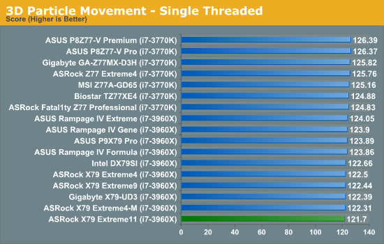
In single threaded performance, there is a clear separation between Z77 and X79, though not by much. ASRock's algorithm for ramping up the CPU speed seems a little flawed, as their boards tend to fall towards the bottom of the rankings.
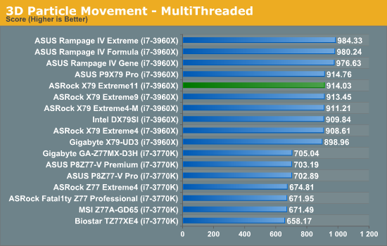
In terms of multithreaded performance, the ASRock X79 Extreme11 takes a standard place for a non-MCE enabled X79 board.
WinRAR x64 3.93 - link
With 64-bit WinRAR, we compress the set of files used in the USB speed tests. WinRAR x64 3.93 attempts to use multithreading when possible, and provides as a good test for when a system has variable threaded load. If a system has multiple speeds to invoke at different loading, the switching between those speeds will determine how well the system will do.
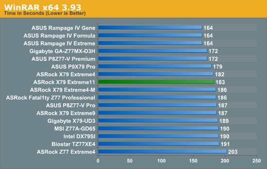
Due to the variable multithreaded nature of WinRAR, MCE enabled boards and those with aggressive ratio changing setting do well here. The ASRock X79 Extreme11 in contrast sits in the middle of the pack.
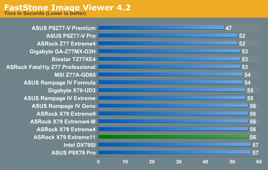
FastStone Image Viewer 4.2 - link
FastStone Image Viewer is a free piece of software I have been using for quite a few years now. It allows quick viewing of flat images, as well as resizing, changing color depth, adding simple text or simple filters. It also has a bulk image conversion tool, which we use here. The software currently operates only in single-thread mode, which should change in later versions of the software. For this test, we convert a series of 170 files, of various resolutions, dimensions and types (of a total size of 163MB), all to the .gif format of 640x480 dimensions.
Xilisoft Video Converter
With XVC, users can convert any type of normal video to any compatible format for smartphones, tablets and other devices. By default, it uses all available threads on the system, and in the presence of appropriate graphics cards, can utilize CUDA for NVIDIA GPUs as well as AMD APP for AMD GPUs. For this test, we use a set of 32 HD videos, each lasting 30 seconds, and convert them from 1080p to an iPod H.264 video format using just the CPU. The time taken to convert these videos gives us our result.
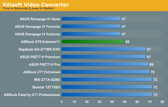
As XVC loves cores and MHz speed, so X79 with a 6C/12T CPU beats all Z77 and 4C/8T CPUs, and MCE wins out. Though the ASRock only loses 3 seconds to the ROG boards, showcasing that for a workstation based on CPU performance, X79 is the top choice.
x264 HD Benchmark
The x264 HD Benchmark uses a common HD encoding tool to process an HD MPEG2 source at 1280x720 at 3963 Kbps. This test represents a standardized result which can be compared across other reviews, and is dependant on both CPU power and memory speed. The benchmark performs a 2-pass encode, and the results shown are the average of each pass performed four times.
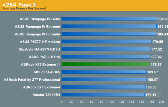
The variable nature of the first pass of our test shows that MHz counts more than cores - MCE enabled boards win here.
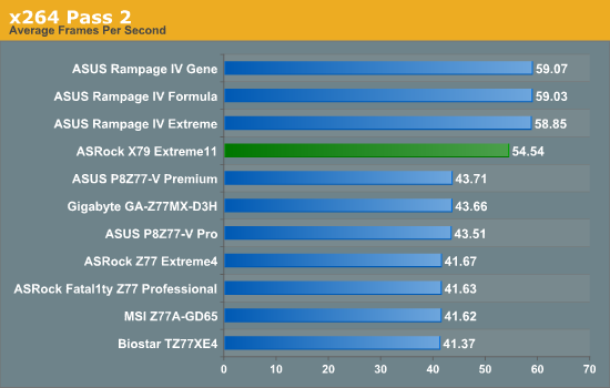
The second pass in contrast loves cores and MHz, with distinct separation between X79 and Z77, the separation between MCE and non-MCE boards.
PCIe 3.0 vs. PCIe 2.0
As part of our testing on the X79 Extreme11, we decided to test both PCIe 2.0 and PCIe 3.0 scenarios. Due to the PLX chips onboard giving us a full x16/x16/x16/x16 minus any PLX latency, it should give a rough idea of how these two technologies perform. Our testing incorporated each benchmark at 2560x1440 using full eye candy settings. Here are our results, indicated by percentage difference of PCIe 3.0 over PCIe 2.0:
|
PCIe 3.0 vs. PCIe 2.0 2560x1440, Full AA/AF ASRock X79 Extreme11 x16/x16/x16/x16 |
||
| Metro 2033 | Dirt3 | |
| 1x 7970 | -0.3% | +3.8% |
| 2x 7970 | +2.6% | +4.3% |
| 3x 7970 | +1.2% | +4.2% |
| 4x 7970 | +1.9% | +0.5% |
As we can see, there is an improvement for Dirt3 and Metro2033, though the difference is barely noticable. The effect of PCIe 3.0 depends on the different engines using DirectX and OpenGL – each system, and thus each gaming engine, uses the PCIe bus differently. In the games where the PCIe bus is used extensively, then PCIe 3.0 will win out. Otherwise we are at the whim of statistical variation between runs.
Dirt 3
Dirt 3 is a rallying video game and the third in the Dirt series of the Colin McRae Rally series, developed and published by Codemasters. Using the in game benchmark, Dirt 3 is run at 2560x1440 with full graphical settings. Results are reported as the average frame rate across four runs.
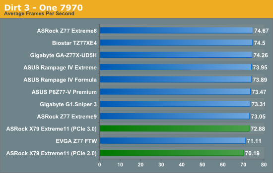
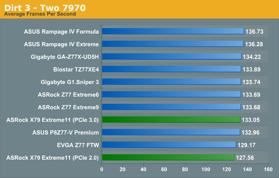
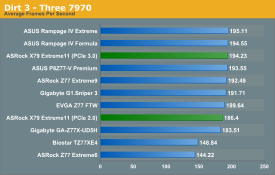
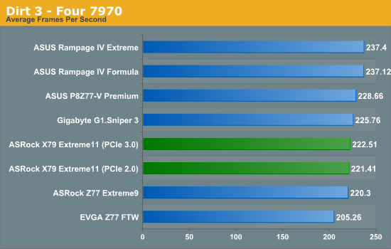
Due to the PLX chips, we would expect the X79 Extreme11 to fall behind slightly in single and dual GPU performance, which is confirmed in the benchmark results. In four-way GPU however, the X79 board falls behind some Z77 boards.
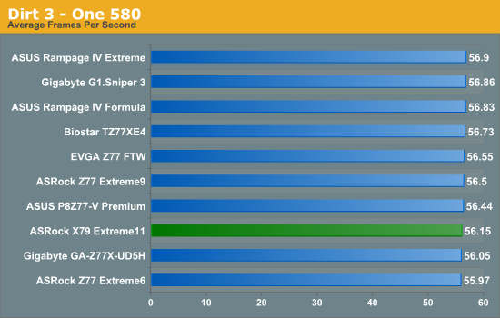
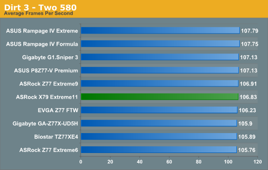
Using NVIDIA GPUs, Dirt3 is still agnostic to any CPU or PCIe performance.
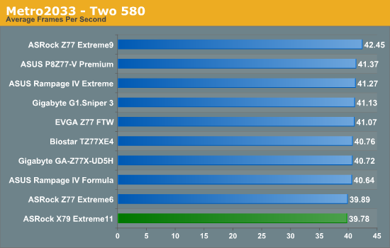
Metro2033
Metro2033 is a DX11 benchmark that challenges every system that tries to run it at any high-end settings. Developed by 4A Games and released in March 2010, we use the inbuilt DirectX 11 Frontline benchmark to test the hardware at 2560x1440 with full graphical settings. Results are given as the average frame rate from 4 runs.
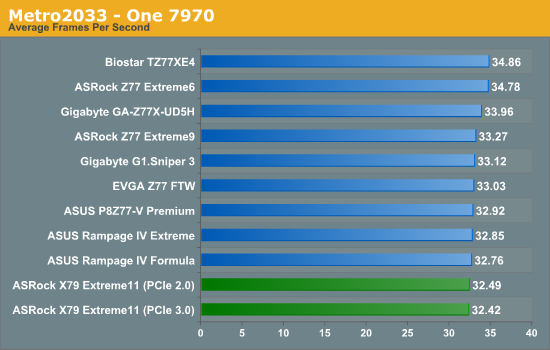
Metro 2033 mirrors similar findings from Dirt3 - the ASRock cannot keep pace with the other boards. This must suggest that having dual PLX chips offers a much bigger hit to frame rates than previously thought.
Testing the LSI SAS 2308 PCIe Controller
As part of this review, ASRock were kind enough to provide a set of eight ADATA XPG SX910 256GB drives in order to test the LSI SAS/SATA ports on the motherboard. These drives are rated for 500 MBps+ sequential read and write speeds, and are based on the LSI SF-2281 controller. Due to the routing of the LSI chip via PCIe 3.0 lanes, our bandwidth ceiling is lifted as we do not have to go via the chipset.
The LSI SAS controller supports SAS2 and SATA 6 Gbps drives. This is in comparison to the C60x server based chipsets for Sandy Bridge-E and Xeon processors based on the 2011 socket, which allow for up to eight SAS/SATA drives limited to SATA 3 Gbps and chipset throughput.
The LSI controller allows for RAID 0, 1 and 10 only, which is a little odd. I would have expected some users to require RAID 5 or 6. Running eight drives in RAID 0 is a unique real world scenario, due to the fail rate potentially wiping all the data, but it does allow us to study peak throughput. Thus the preferred scenario here will be RAID 10 across eight drives, thus taking advantage of striping across 4 of the drives but also having them mirrored.
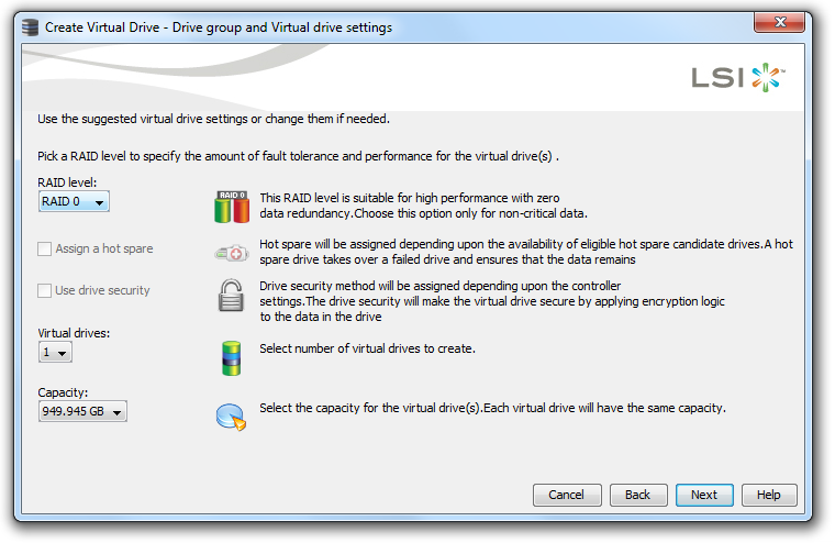
The LSI platform is very easy to use. With the drives plugged in and powered (I had to rummage for suitable power connectors), the LSI software provided (MegaRAID) on the ASRock Driver DVD is loaded and run. After a login screen, we are presented with the following:
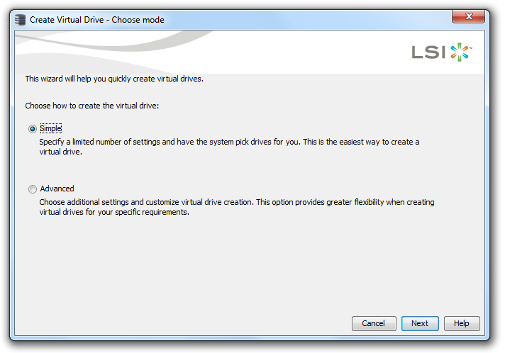
In order to create array, we select the ‘Create Virtual Drive’ option. We then get an option to select either an Easy mode for creating the virtual drive, or an advanced mode. Both are very limited in their options, especially as we can only choose one stripe size – 64KB.
The virtual drive then needs to be mounted in Windows, using the Disk Management tool.
The LSI chip by default is set to run in PCIe 3.0 mode in the BIOS. There is also an option to allow booting from the LSI chip, via Port 7. This unfortunately adds a large amount of time to the booting of the system, around 40-50 more seconds.
With this in mind, we tested several scenarios for bandwidth and 4K performance with the LSI chip. As the LSI has no access to additional cache like a PCIe card, we will see that the peak performance lies more in bulk sequential transfers, rather than small transfers.
For the tests, we used the standard ATTO benchmark and the following scenarios in RAID-0:
LSI Chip with 1, 2, 3, 4, 5, 6, 7, 8 drives (listed as SAS x) via MegaRAID
Chipset with 1, 2 drives on SATA 6 Gbps (listed as x+0)
Chipset with 1, 2, 3, 4 drives on SATA 3 Gbps (listed as (0+x)
Chipset with 1 drive on SATA 6 Gbps and 1, 2, 3, 4 drives on SATA 3 Gbps (listed as 1+x)
Chipset with 2 drives on SATA 6 Gbps and 1, 2, 3, 4 drives on SATA 3 Gbps (listed as 2+x)
All chipset scenarios were set using the RAID from BIOS rather than in the OS.
In terms of peak speeds using ATTO, we recorded the following results:
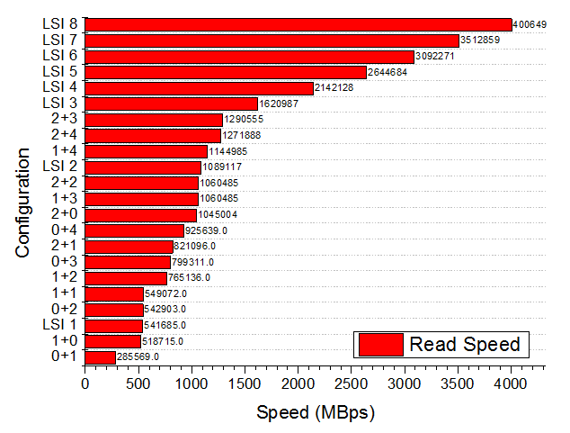
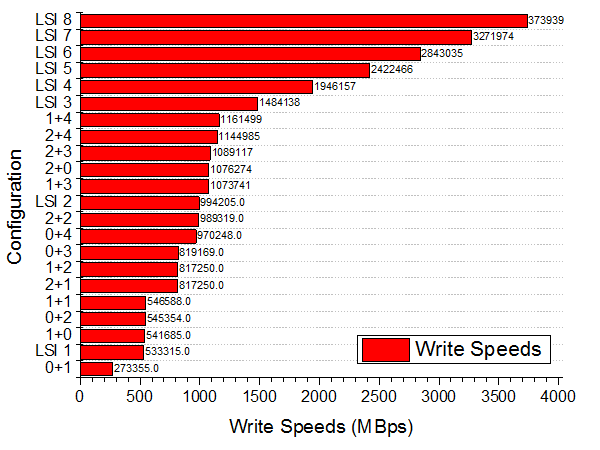
There are plenty of conclusions to draw from this – for peak throughput, the LSI ports are preferred. When using the chipset connections, going from 2+0 to 2+1 will bring a drop in performance. Also worthy of note is our top speed with eight drives in RAID-0 – we hit 4.0 GBps read and 3.72 GBps write. We can see more by looking at how the chipset deals with reads and writes differently to the LSI chip:
In terms of write speeds, all the drive configurations perform nearly the same until the advantage of more drives takes over, and the LSI configurations of 3+ pull ahead. However, in the read speeds, all the chipset configurations that feature at least one SATA 6 Gbps drive have distinctly better read speeds below 64 KB transfer size. This could be due to some chipset caching or clever manipulation of the data. Thus for standard OS drives, putting two drives on the chipset SATA 6 Gbps ports will be more beneficial than using the LSI chip.
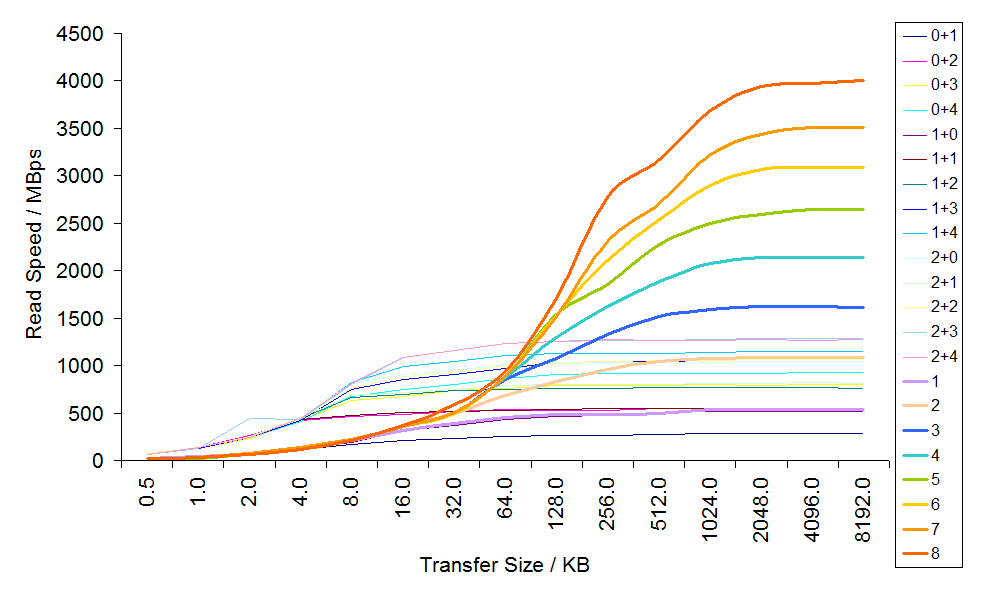
In terms of scaling, the LSI chip has the following 3D surfaces for read and write:
In both read and write, we only see any relevant scaling of drives beyond 128KB transfers. The large the transfer, the more the scaling becomes almost 1:1 as more drives are added.
Ultimately though, this may not be the best use case scenario for the product. As mentioned above, perhaps an eight drive RAID 10 array could be utilized with SAS drives, whereby the drive is more relevant to the speed than the port is (despite ASRock advertising stating peak throughputs).
ASRock X79 Extreme11
To conclude, it is hard to judge a motherboard like the ASRock X79 Extreme11. With no other major competing products offering similar functionality, ASRock can charge a pretty penny for the product. However, does it still retain the usefulness or bang for buck in terms of performance?
For your $600 of green, the main selling point is the X79 platform mixed with two PLX PEX 8747 chips which allow four PCIe devices to be run at x16/x16/x16/x16 in PCIe 3.0 or up to seven devices to be run at x16/x8/x8/x8/x8/x8/x8 also in PCIe 3.0. This combination leaves eight PCIe 3.0 lanes from the CPU, which are directed straight into an LSI SAS 2308 PCIe 3.0 RAID controller. This LSI chip gives eight ports capable of SAS2/SATA 6 Gbps speeds, in RAID 0, 1 or 10 configurations. An equivalent PCIe 3.0 card would set a user back several hundred as well as taking up a PCIe slot.
On top of the PLX and LSI chips, we also get a full-bodied X79 motherboard, featuring eight memory slots, dual Broadcom NIC capable of Teaming/Link Aggregation, a Creative Core3D sound chip, enhanced power delivery, and eight USB 3.0 ports via TI controllers. Software comes in the XFast flavors, with XFast RAM taking advantage of the ability of X79 to hold more memory. The board itself is also supports a multitude of Xeon processors, as well as ECC memory with the Xeons. There is a good amount in the box too, such as six SATA cables and a USB 3.0 panel, but it should be noted that this internal bundle is similar to cheaper ASRock products. The only thing missing in my opinion would be a WiFi connection on the IO, similar to that done by ECS.
Performance wise, the X79 Extreme11 does not win many accolades. It performs similarly or worse than other X79 motherboards in the market - in our GPU testing, the board continuously came near the bottom. The separation ASRock likes to make with the X79 Extreme11 is the PCIe functionality and the ability to include SAS drives on board - the speed of the extra ports reached a staggering 4.0 GBps, even though that may not be a realistic use scenario. The extra ports also are a little hampered by not having additional cache to help with writing short transfer sizes like on a PCIe card.
With our testing, and the price range of this motherboard, it is safe to say that this product is more aimed at workstation projects, such as an 8-core Xeon with ECC, rather than a product for gamers or overclockers. Tool it up with eight SAS drives, seven single slot GPUs, and away you go with a nice number crunching machine. Instead of paying in terms of price for performance, we are all talking about price for functionality here.
As a technical exercise, what ASRock have done is pretty amazing. In terms of pure innovation in a relatively stagnant market, I have to award the ASRock X79 Extreme11 a bronze award for pushing boundaries and enabling innovation in the motherboard market. This motherboard, paired with a deep wallet, could be a number crunching machine for video or audio enthusiasts, or GPU crunchers who yearn PCIe bandwidth but also SAS compatibility. This is strictly an enthusiast’s motherboard.

ASRock X79 Extreme11
AnandTech Editor’s Choice Bronze Award


