Original Link: https://www.anandtech.com/show/6936/intels-silvermont-architecture-revealed-getting-serious-about-mobile
Intel’s Silvermont Architecture Revealed: Getting Serious About Mobile
by Anand Lal Shimpi on May 6, 2013 1:00 PM EST- Posted in
- CPUs
- Intel
- Silvermont
- SoCs
The most frustrating part about covering Intel’s journey into mobile over the past five years is just how long it’s taken to get here. The CPU cores used in Medfield, Clover Trail and Clover Trail+ are very similar to what Intel had with the first Atom in 2008. Obviously we’re dealing with higher levels of integration and tweaks for further power consumption, but the architecture and much of the core remains unchanged. Just consider what that means. A single Bonnell core, designed in 2004, released in 2008, is already faster than ARM’s Cortex A9. Intel had this architecture for five years now and from the market’s perspective, did absolutely nothing with it. You could argue that the part wasn’t really ready until Intel had its 32nm process, so perhaps we’ve only wasted 3 years (Intel debuted its 32nm process in 2010). It’s beyond frustrating to think about just how competitive Intel would have been had it aggressively pursued this market.
Today Intel is in a different position. After acquisitions, new hires and some significant internal organizational changes, Intel seems to finally have the foundation to iterate and innovate in mobile. Although Bonnell (the first Atom core) was the beginning of Intel’s journey into mobile, it’s Silvermont - Intel’s first new Atom microarchitecture since 2008 - that finally puts Intel on the right course.
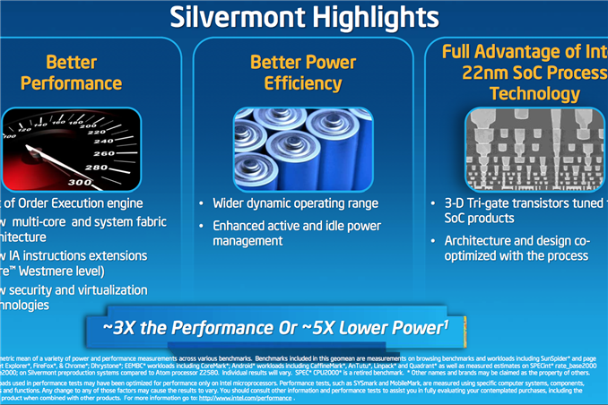
Although Silvermont can find its way into everything from cars to servers, the architecture is primarily optimized for use in smartphones and then in tablets, in that order. This is a significant departure from the previous Bonnell core that was first designed to serve the now defunct Mobile Internet Devices category that Intel put so much faith in back in the early to mid 2000s. As Intel’s first Atom architecture designed for mobile, expectations are high for Silvermont. While we’ll have to wait until the end of the year to see Silvermont in tablets (and early next year for phones), the good news for Intel is that Silvermont seems competitive right out of the gate. The even better news is that Silvermont will only be with us for a year before it gets its first update: Airmont.
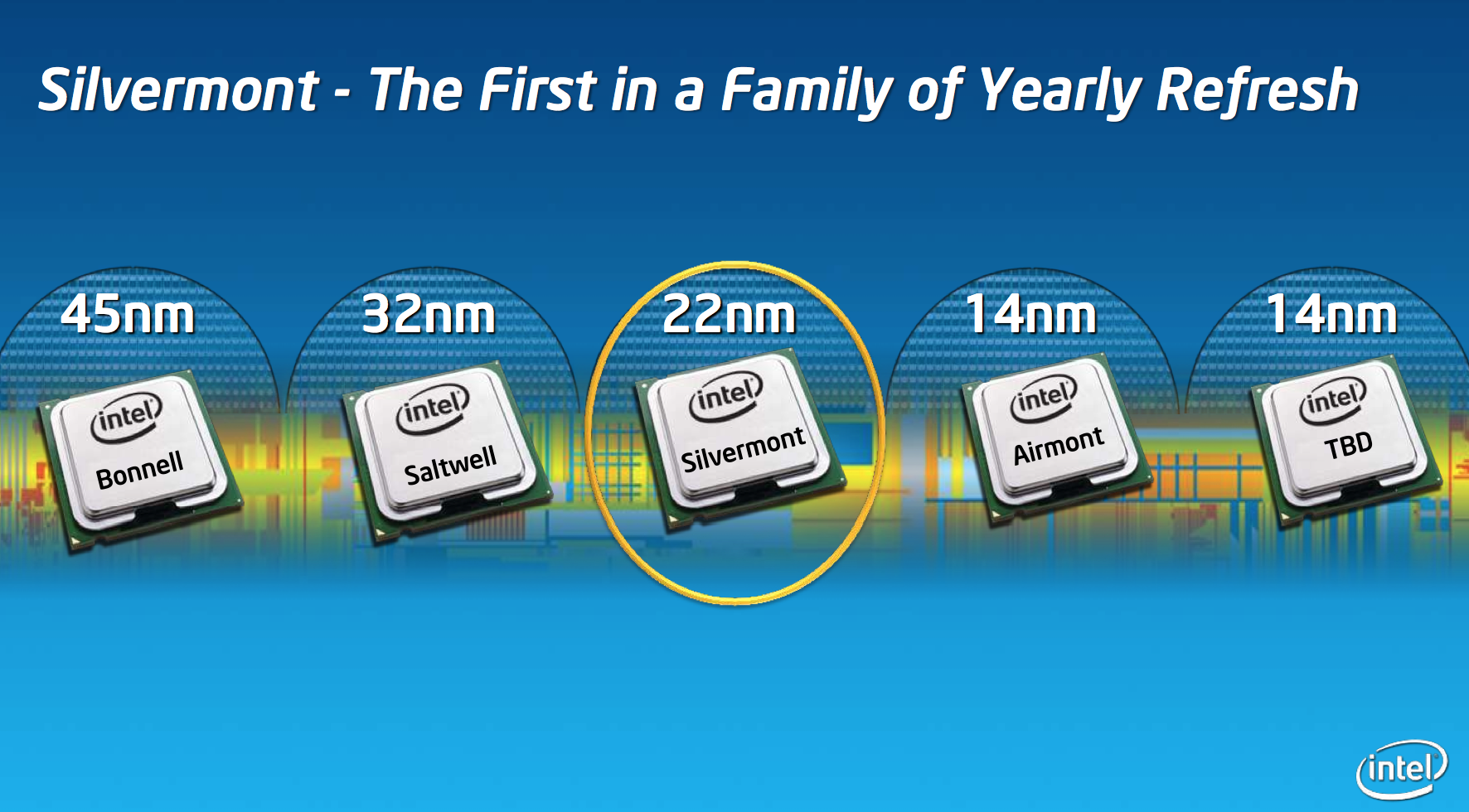 Intel made this announcement last year, but Silvermont is the beginning of Intel’s tick-tock cadence for Atom. Intel plans on revving Atom yearly for at least the next three years. Silvermont introduces a new architecture, while Airmont will take that architecture and bring it down to 14nm in 2014/2015. One year later, we’ll see another brand new architecture take the stage also on 14nm. This is a shift that Intel needed to implement years ago, but it’s still not too late.
Before we get into an architectural analysis of Silvermont, it’s important to get some codenames in order. Bonnell was the name of the original 45nm Atom core, it was later shrunk to 32nm and called Saltwell when it arrived in smartphones and tablets last year. Silvermont is the name of the CPU core alone, but when it shows up in tablets later this year it will do so as a part of the Baytrail SoC and a part of the Merrifield SoC next year in smartphones.
22nm
To really understand the Silvermont story, you need to first understand Intel’s 22nm SoC process. Two years ago Intel announced its 22nm tri-gate 3D transistors, which would eventually ship a year later in Intel’s Ivy Bridge processors. That process wasn’t suited for ultra mobile. It was optimized for the sort of high performance silicon that was deployed on it, but not the ultra compact, very affordable, low power silicon necessary in smartphones and tablets. A derivative of that process would be needed for mobile. Intel now makes two versions of all of its processes, one optimized for its high performance CPUs and one for low power SoCs. P1270 was the 22nm CPU process, and P1271 is the low power SoC version. Silvermont uses P1271. The high level characteristics are the same however. Intel’s 22nm process moves to tri-gate non-planar transistors that can significantly increase transistor performance and/or decrease power.

This part is huge. The move to 22nm 3D transistors lets Intel drop threshold voltage by approximately 100mV at the same leakage level. Remember that power scales with the square of voltage, so a 100mV savings depending on what voltage you’re talking about can be very huge. Intel’s numbers put the power savings at anywhere from 25 - 35% at threshold voltage. The gains don’t stop there either. At 1V, Intel’s 22nm process gives it an 18% improvement in transistor performance or at the same performance Intel can run the transistors at 0.8V - a 20% power savings. The benefits are even more pronounced at lower voltages: 37% faster performance at 0.7V or less than half the active power at the same performance.
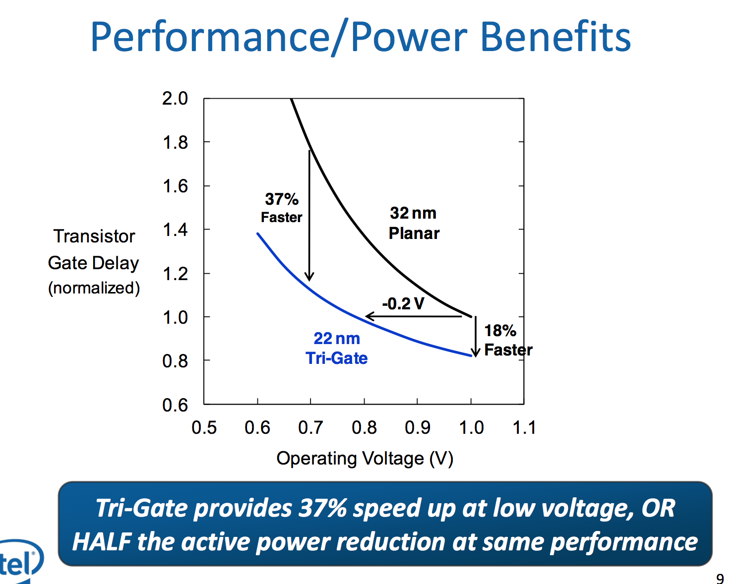
The end result here is Intel can scale frequency and/or add more active logic without drawing any more power than it did at 32nm. This helps at the top end with performance, but the vast majority of the time mobile devices are operating at very lower performance and power levels. Where performance doesn’t matter as much, Intel’s 22nm process gives it an insane advantage.
If we look back at our first x86 vs. ARM performance data we get a good indication of where Intel’s 32nm process had issues and where we should see tangible improvements with the move to 22nm:
Qualcomm’s 28nm Krait 200 was actually able to get down to lower power levels than Intel could at 32nm. Without having specific data I can’t say for certain, but it’s extremely likely that with Silvermont Intel will be able to drive down to far lower power levels than anything we’ve ever measured.
Understanding what Intel’s 22nm process gives it is really key to understanding Silvermont.
OoOE
You’re going to come across the phrase out-of-order execution (OoOE) a lot here, so let’s go through a quick refresher on what that is and why it matters.
At a high level, the role of a CPU is to read instructions from whatever program it’s running, determine what they’re telling the machine to do, execute them and write the result back out to memory.
The program counter within a CPU points to the address in memory of the next instruction to be executed. The CPU’s fetch logic grabs instructions in order. Those instructions are decoded into an internally understood format (a single architectural instruction sometimes decodes into multiple smaller instructions). Once decoded, all necessary operands are fetched from memory (if they’re not already in local registers) and the combination of instruction + operands are issued for execution. The results are committed to memory (registers/cache/DRAM) and it’s on to the next one.
In-order architectures complete this pipeline in order, from start to finish. The obvious problem is that many steps within the pipeline are dependent on having the right operands immediately available. For a number of reasons, this isn’t always possible. Operands could depend on other earlier instructions that may not have finished executing, or they might be located in main memory - hundreds of cycles away from the CPU. In these cases, a bubble is inserted into the processor’s pipeline and the machine’s overall efficiency drops as no work is being done until those operands are available.
Out-of-order architectures attempt to fix this problem by allowing independent instructions to execute ahead of others that are stalled waiting for data. In both cases instructions are fetched and retired in-order, but in an OoO architecture instructions can be executed out-of-order to improve overall utilization of execution resources.
The move to an OoO paradigm generally comes with penalties to die area and power consumption, which is one reason the earliest mobile CPU architectures were in-order designs. The ARM11, ARM’s Cortex A8, Intel’s original Atom (Bonnell) and Qualcomm’s Scorpion core were all in-order. As performance demands continued to go up and with new, smaller/lower power transistors, all of the players here started introducing OoO variants of their architectures. Although often referred to as out of order designs, ARM’s Cortex A9 and Qualcomm’s Krait 200/300 are mildly OoO compared to Cortex A15. Intel’s Silvermont joins the ranks of the Cortex A15 as a fully out of order design by modern day standards. The move to OoO alone should be good for around a 30% increase in single threaded performance vs. Bonnell.
Pipeline
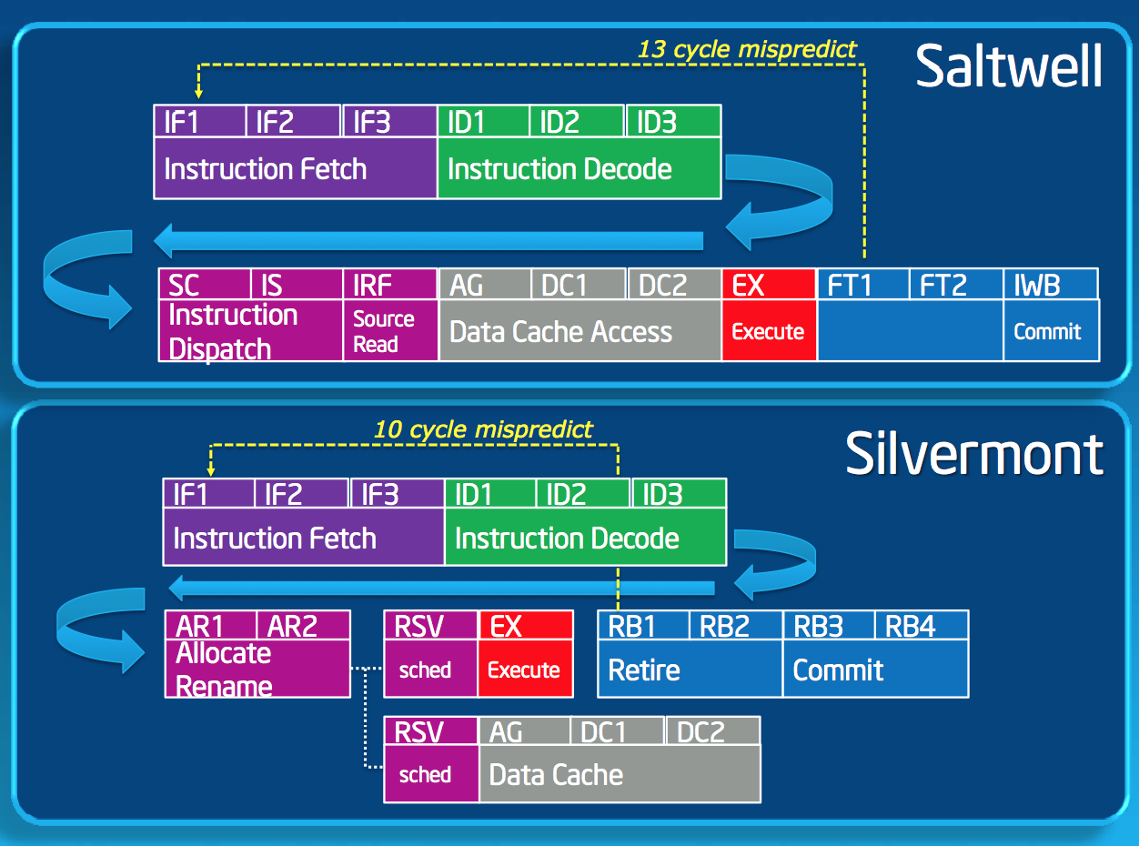
Silvermont changes the Atom pipeline slightly. Bonnell featured a 16 stage in-order pipeline. One side effect to the design was that all operations, including those that didn’t have cache accesses (e.g. operations whose operands were in registers), had to go through three data cache access stages even though nothing happened during those stages. In going out-of-order, Silvermont allows instructions to bypass those stages if they don’t need data from memory, effectively shortening the mispredict penalty from 13 stages down to 10. The integer pipeline depth now varies depending on the type of instruction, but you’re looking at a range of 14 - 17 stages.
Branch prediction improves tremendously with Silvermont, a staple of any progressive microprocessor architecture. Silvermont takes the gshare branch predictor of Bonnell and significantly increased the size of all associated data structures. Silvermont also added an indirect branch predictor. The combination of the larger predictors and the new indirect predictor should increase branch prediction accuracy.
Couple better branch prediction with a lower mispredict latency and you’re talking about another 5 - 10% increase in IPC over Bonnell.
Sensible Scaling: OoO Atom Remains Dual-Issue
The architectural progression from Apple, ARM and Qualcomm have all been towards wider, out-of-order cores, to varying degrees. With Swift and Krait, Apple and Qualcomm both went wider. From Cortex A8 to A9 ARM went OoO and then from A9 to A15 ARM introduced a significantly wider architecture. Intel bucks the trend a bit by keeping the overall machine width unchanged with Silvermont. This is still a 2-wide architecture.
At the risk of oversimplifying the decision here, Intel had to weigh die area, power consumption as well as the risk of making Atom too good when it made the decision to keep Silvermont’s design width the same as Bonnell. A wider front end would require a wider execution engine, and Intel believed it didn’t need to go that far (yet) in order to deliver really good performance.
Keeping in mind that Intel’s Bonnell core is already faster than ARM’s Cortex A9 and Qualcomm’s Krait 200, if Intel could get significant gains out of Silvermont without going wider - why not? And that’s exactly what’s happened here.
If I had to describe Intel’s design philosophy with Silvermont it would be sensible scaling. We’ve seen this from Apple with Swift, and from Qualcomm with the Krait 200 to Krait 300 transition. Remember the design rule put in place back with the original Atom: for every 2% increase in performance, the Atom architects could at most increase power by 1%. In other words, performance can go up, but performance per watt cannot go down. Silvermont maintains that design philosophy, and I think I have some idea of how.
Previous versions of Atom used Hyper Threading to get good utilization of execution resources. Hyper Threading had a power penalty associated with it, but the performance uplift was enough to justify it. At 22nm, Intel had enough die area (thanks to transistor scaling) to just add in more cores rather than rely on HT for better threaded performance so Hyper Threading was out. The power savings Intel got from getting rid of Hyper Threading were then allocated to making Silvermont an out-of-order design, which in turn helped drive up efficient use of the execution resources without HT. It turns out that at 22nm the die area Intel would’ve spent on enabling HT was roughly the same as Silvermont’s re-order buffer and OoO logic, so there wasn’t even an area penalty for the move.
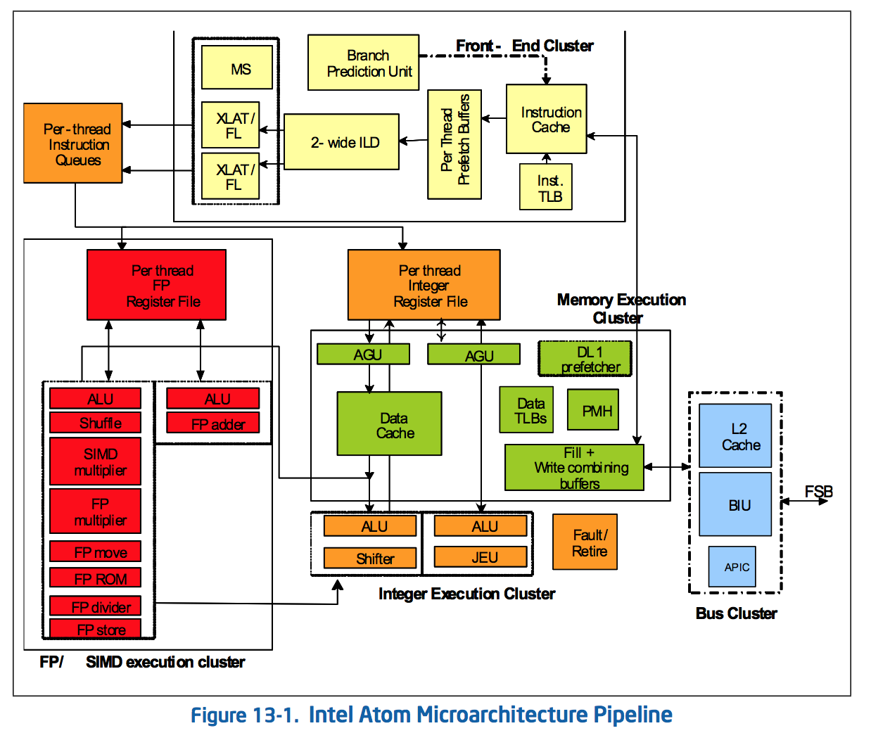
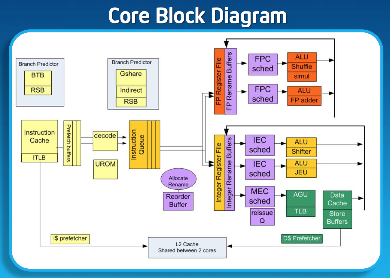
The Original Atom microarchitecture
Remaining a 2-wide architecture is a bit misleading as the combination of the x86 ISA and treating many x86 ops as single operations down the pipe made Atom physically wider than its block diagram would otherwise lead you to believe. Remember that with the first version of Atom, Intel enabled the treatment of load-op-store and load-op-execute instructions as single operations post decode. Instead of these instruction combinations decoding into multiple micro-ops, they are handled like single operations throughout the entire pipeline. This continues to be true in Silvermont, so the advantage remains (it also helps explain why Intel’s 2-wide architecture can deliver comparable IPC to ARM’s 3-wide Cortex A15).
While Silvermont still only has two x86 decoders at the front end of the pipeline, the decoders are more capable. While many x86 instructions will decode directly into a single micro-op, some more complex instructions require microcode assist and can’t go through the simple decode paths. With Silvermont, Intel beefed up the simple decoders to be able to handle more (not all) microcoded instructions.
Silvermont includes a loop stream buffer that can be used to clock gate fetch and decode logic in the event that the processor detects it’s executing the same instructions in a loop.
Execution
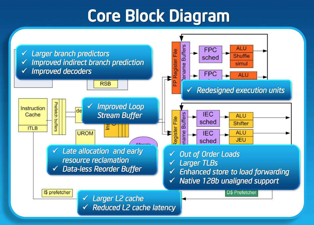
Silvermont’s execution core looks similar to Bonnell before it, but obviously now the design supports out-of-order execution. Silvermont’s execution units have been redesigned to be lower latency. Some FP operations are now quicker, as well as integer multiplies.
Loads can execute out of order. Don’t be fooled by the block diagram, Silvermont can issue one load and one store in parallel.
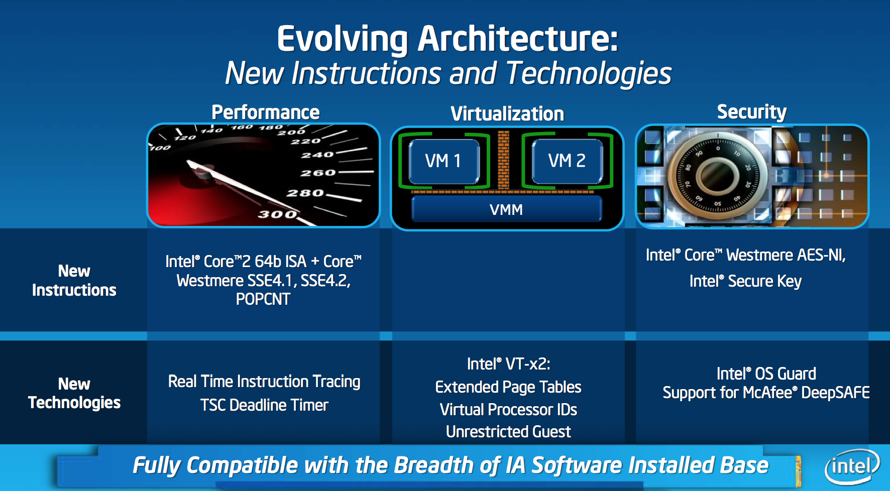
ISA
The original Atom processor enabled support for Merom/Conroe-class x86 instructions, it lacked SSE4 support due to die/power constraints; that was at 45nm, at 22nm there’s room for improvement. Silvermont brings ISA compatibility up to Westmere levels (Intel’s 2010 Core microprocessor architecture). There’s now support for SSE4.1, SSE4.2, POPCNT and AES-NI.
Silvermont is 64-bit capable, although it is up to Intel to enable 64-bit support on various SKUs similar to what we’ve seen with Atom thus far.
IPC and Frequency
The combination of everything Intel is doing on the IPC front give it, according to Intel, roughly the same single threaded performance as ARM’s Cortex A15. We’ve already established that the Cortex A15 is quite good, but here’s where Silvermont has a chance to pull ahead. We already established that Intel’s 22nm process can give it anywhere from a 18 - 37% performance uplift at the same power consumption. IPC scaling gives Silvermont stable footing, but the ability to run at considerably higher frequencies without drawing more power is what puts it over the top.
Intel isn’t talking about frequencies at this point, but I’ve heard numbers around 2 - 2.4GHz thrown around a lot. Compared to the 1.6 - 2GHz range we currently have with Bonnell based silicon, you can see how the performance story gets serious quickly. Intel is talking about a 50% improvement in IPC at the core, combine that with a 30% improvement in frequency without any power impact and you’re now at 83% better performance potentially with no power penalty. There are other advantages at the SoC level that once factored in drive things even further.
Real Turbo Modes & Power Management
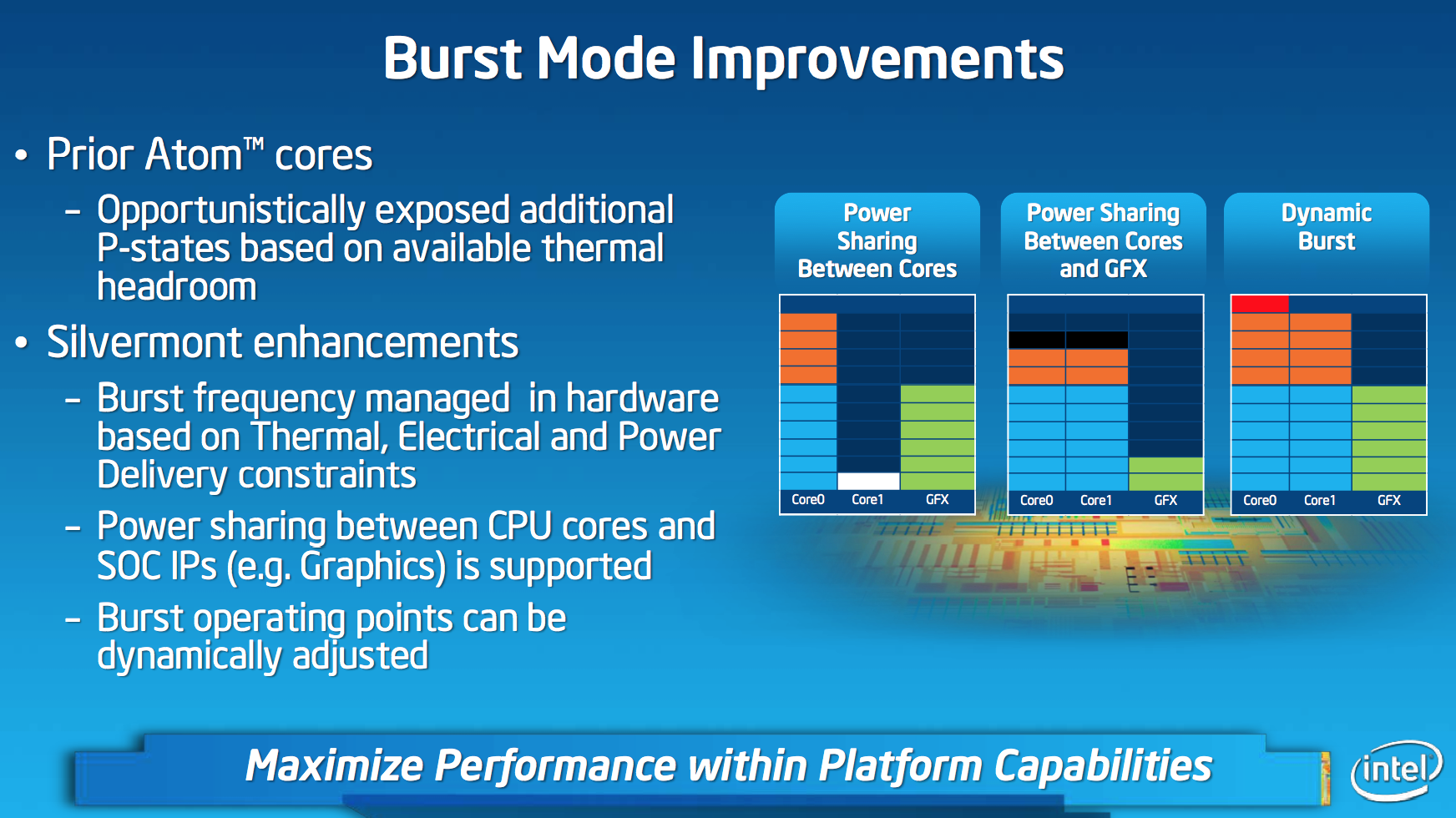
Previous Atom based mobile SoCs had a very crude version of Intel’s Turbo Boost. The CPU would expose all of its available P-states to the OS and as it became thermally limited, Intel would clamp the max P-state it would expose to the OS. Everything was OS-driven and previous designs weren’t able to capitalize on unused thermal budget elsewhere in the SoC to drive up frequency in active parts of chip. This lack of flexibility even impacted the SoC at the CPU core level. When running a single threaded app, Medfield/Clover Trail/et al couldn’t take thermal budget freed up by the idle core and use it to drive the frequency of the active core. Previous Atom implementations were basically somewhere in the pre-Nehalem era of thermal/boost management. From what I’ve seen, this is also how a lot of the present day ARM architectures work as well. At best, they vary what operating states they expose to the OS and clamp max frequency depending on thermals. To the best of my knowledge, none of the SoC vendors today actively implement modern big-core-Intel-like frequency management. Silvermont fixes this.
Silvermont, like Nehalem and the architectures that followed, gets its own power control unit that monitors thermals and handles dynamic allocation of power budget to various blocks within the SoC. If I understand this correctly, Silvermont should expose a maximum base frequency to the OS but depending on instruction mix and available TDP it can turbo up beyond that maximum frequency as long as it doesn’t exceed TDP. Like Sandy Bridge, Silvermont will even be able to exceed TDP for a short period of time if the package temperature is low enough to allow it. Finally, Silvermont’s turbo can also work across IP blocks: power budget allocated to the GPU can be transferred to the CPU cores (and vice versa).
By big-core standards (especially compared to Haswell), Silvermont’s turbo isn’t all that impressive but compared to how things are currently handled in the mobile space this should be a huge step forward.
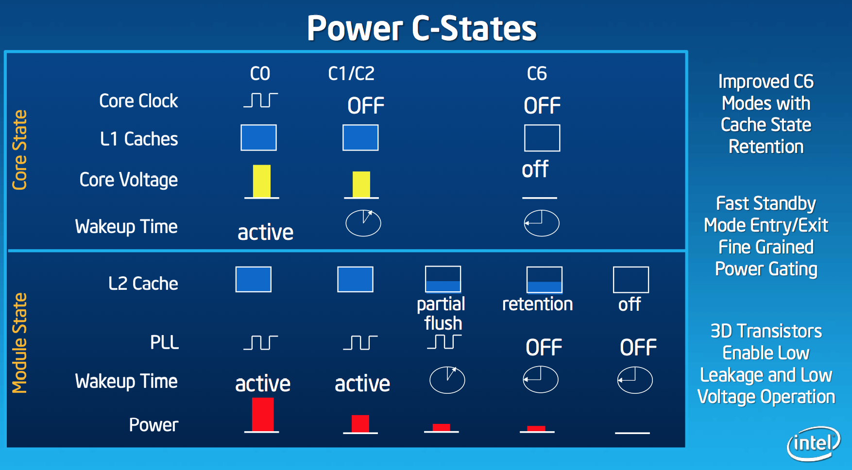
On the power management side, getting in and out of C6 should be a bit quicker. There's also a new C6 mode with cache state retention.
The Silvermont Module and Caches
Like AMD’s Bobcat and Jaguar designs, Silvermont is modular. The default Silvermont building block is a two-core/two-thread design. Each core is equally capable and there’s no shared execution hardware. Silvermont supports up to 8-core configurations by placing multiple modules in an SoC.
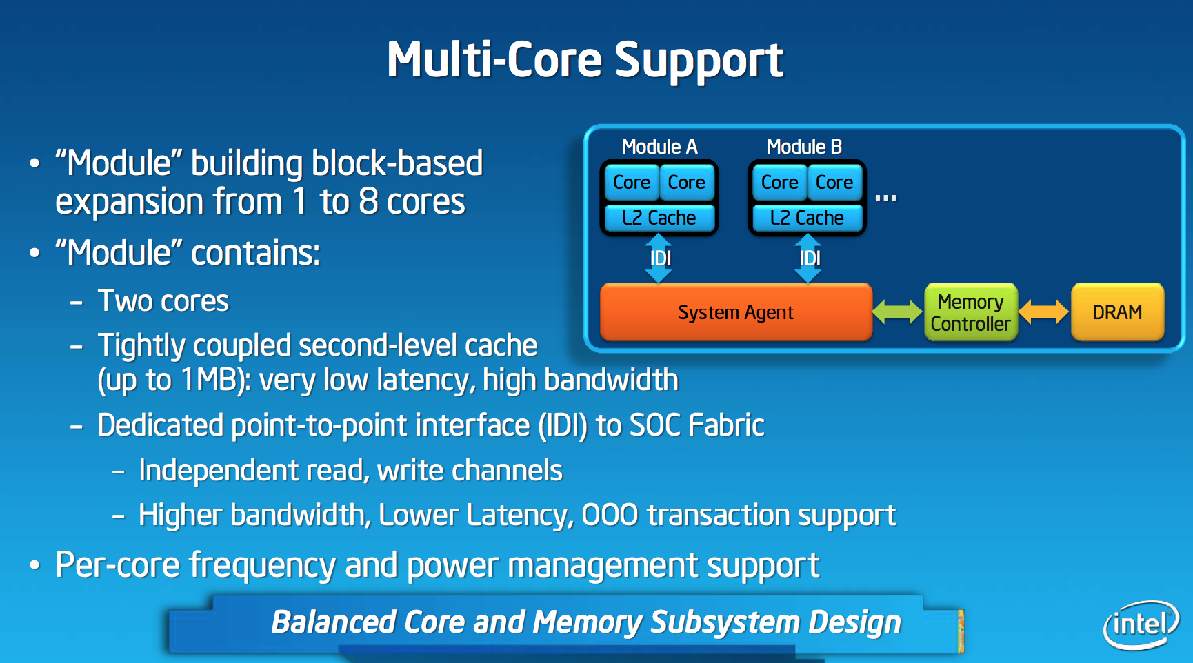
Each module features a shared 1MB L2 cache, a 2x increase over the core:cache ratio of existing Atom based processors. Despite the larger L2, access latency is reduced by 2 clocks. The default module size gives you clear indication as to where Intel saw Silvermont being most useful. At the time of its inception, I doubt Intel anticipated such a quick shift to quad-core smartphones otherwise it might’ve considered a larger default module size.
L1 cache sizes/latencies haven’t changed. Each Silvermont core features a 32KB L1 data cache and 24KB L1 instruction cache.
Silvermont Supports Independent Core Frequencies: Vindication for Qualcomm?
In all Intel Core based microprocessors, all cores are tied to the same frequency - those that aren’t in use are simply shut off (power gated) to save power. Qualcomm’s multi-core architecture has always supported independent frequency planes for all CPUs in the SoC, something that Intel has always insisted was a bad idea. In a strange turn of events, Intel joins Qualcomm in offering the ability to run each core in a Silvermont module at its own independent frequency. You could have one Silvermont core running at 2.4GHz and another one running at 1.2GHz. Unlike Qualcomm’s implementation, Silvermont’s independent frequency planes are optional. In a split frequency case, the shared L2 cache always runs at the higher of the two frequencies. Intel believes the flexibility might be useful in some low cost Silvermont implementations where the OS actively uses core pinning to keep threads parked on specific cores. I doubt we’ll see this on most tablet or smartphone implementations of the design.
From FSB to IDI
Atom and all of its derivatives have a nasty secret: they never really got any latency benefits from integrating a memory controller on die. The first implementation of Atom was a 3-chip solution, with the memory controller contained within the North Bridge. The CPU talked to the North Bridge via a low power Front Side Bus implementation. This setup should sound familiar to anyone who remembers Intel architectures from the late 90s up to the mid 2000s. In pursuit of integration, Intel eventually brought the memory controller and graphics onto a single die. Historically, bringing the memory controller onto the same die as the CPU came with a nice reduction in access latency - unfortunately Atom never enjoyed this. The reasoning? Atom never ditched the FSB interface.
Even though Atom integrated a memory controller, the design logically looked like it did before. Integration only saved Intel space and power, it never granted it any performance. I suspect Intel did this to keep costs down. I noticed the problem years ago but completely forgot about it since it’s been so long. Thankfully, with Silvermont the FSB interface is completely gone.
Silvermont instead integrates the same in-die interconnect (IDI) that is used in the big Core based processors. Intel’s IDI is a lightweight point to point interface that’s far lower overhead than the old FSB architecture. The move to IDI and the changes to the system fabric are enough to improve single threaded performance by low double digits. The gains are even bigger in heavily threaded scenarios.
Another benefit of moving away from a very old FSB to IDI is increased flexibility in how Silvermont can clock up/down. Previously there were fixed FSB:CPU ratios that had to be maintained at all times, which meant the FSB had to be lowered significantly when the CPU was running at very low frequencies. In Silvermont, the IDI and CPU frequencies are largely decoupled - enabling good bandwidth out of the cores even at low frequency levels.
The System Agent
Silvermont gains an updated system agent (read: North Bridge) that’s much better at allowing access to main memory. In all previous generation Atom architectures, virtually all memory accesses had to happen in-order (Clover Trail had some minor OoO improvements here). Silvermont’s system agent now allows reordering of memory requests coming in from all consumers/producers (e.g. CPU cores, GPU, etc...) to optimize for performance and quality of service (e.g. ensuring graphics demands on memory can regularly pre-empt CPU requests when necessary).
SoCs and Graphics
Intel isn’t talking about implementations of Silvermont today other than to say that it will show up in smartphones (Merrifield), tablets (Baytrail), automotive (unannounced), communications infrastructure products (Rangeley) and microservers (Avoton). Baytrail, the tablet implementation of Silvermont, will be available by the end of this year running both Windows 8 (8.1/Blue?) and Android. Silvermont based Merrifield phones will show up early in 2014.
What we know about Baytrail is that it will be a quad-core implementation of Silvermont paired with Intel’s own Gen 7 graphics. Although we don’t know clock speeds, we do know that Baytrail’s GPU core will feature 4 EUs - 1/4 the number used in Ivy Bridge’s Gen7 implementation (Intel HD 4000). Ultimately we can’t know how fast the GPU will be until we know clock speeds, but I wouldn’t be too surprised to see something at or around where the iPad 4’s GPU is today. Given Intel’s recent announcements around Iris and Iris Pro, it’s clear that the mobile team hasn’t yet had the graphics wakeup call that the Core team just got - but I suspect the Atom group will get there sooner rather than later. Intel’s eDRAM approach to scaling Haswell graphics (and CPU) performance has huge implications in mobile. I wouldn’t expect eDRAM enabled mobile SoCs based on Silvermont, but I wouldn’t be too surprised to see something at 14nm.
Penryn-Class Performance
When Atom first came out, I put its CPU performance in perspective by comparing it to older Pentium M based notebooks. It turned out that a 1.6GHz Atom performed similarly to a 1.2GHz Pentium M. So how does Silvermont stack up in PC notebook terms?
On single threaded performance, you should expect a 2.4GHz Silvermont to perform like a 1.2GHz Penryn. To put it in perspective of actual systems, we’re talking about around the level of performance of an 11-inch Core 2 Duo MacBook Air from 2010. Keep in mind, I’m talking about single threaded performance here. In heavily threaded applications, a quad-core Silvermont should be able to bat even further up the Penryn line. Intel is able to do all of this with only a 2-wide machine (lower IPC, but much higher frequency thanks to 22nm).
There’s no doubt in my mind that a Baytrail Android tablet will deliver amazing performance, the real unknown is whether or not a Baytrail Windows 8 detachable/convertible will be fast enough to deliver a good enough legacy Windows experience. I suspect it’ll take Airmont before we really get there by my standards, but it’ll be close this round for sure.
What’ll really be interesting to see is how Silvermont fares in smartphones. Max clock speeds should be lower than what’s possible in a tablet, but not by all that much thanks to good power management. When viewed in that light, I don’t know that there’s a more exciting mobile architecture announced at this point. The ability to deliver 2010 11-inch MacBook Air performance in a phone is insane.
Tablet Expectations
Intel is getting architectural details about Silvermont launch ahead of actual SoCs based on the CPU. Baytrail tablets based on Silvermont cores are currently in development and are expected to show up by the end of the year. The Silvermont story at the end of this year should be a lot better than Clovertrail last year. Windows 8 will be in its second major revision (codename Windows Blue) and Intel will launch with both Android and Windows tablet availability. The inclusion of Android is very important to hitting lower price points, something Clovertrail really didn’t have last year. We should see Baytrail based tablets span the gamut of Nexus 7 to iPad pricing, with Haswell picking up where Silvermont ends.
Form factors should be no thicker than Clovertrail based designs, although it will be possible to go thinner with Baytrail/Silvermont should an OEM decide to. Displays should also be a lot better this time around. Intel is working with some OEMs on color calibration, an important step forward as I’m hearing Qualcomm will be doing the same with Snapdragon 800. We’ll also finally see resolutions higher than 1366x768, including potentially some competition for the iPad with Retina Display. Silvermont’s new system agent should do a good job of prioritizing GPU access to main memory in these ultra high resolution scenarios.
Performance
With tablets still months away from being production ready, there’s nothing for us to publicly test. Intel did share some of its own numbers off of its Baytrail reference tablet however, and they are impressive.
All of the Intel comparisons report the geometric mean performance advantage over a spectrum of benchmarks. The benchmarks used include SPECint2K, CoreMark, SunSpider, web page load tests in IE/Chrome/Firefox, Linpack, AnTuTu and Quadrant (ugh) among others. The point here isn’t to demonstrate absolute peak performance in one benchmark, but to instead give us a general idea of the sorts of gains we should expect to see from Silvermont/Baytrail tablets vs the competition. It’s an admirable effort and honestly the right way to do things (short of actually giving us a pre-production tablet to test that is). We’ll start with a comparison to Saltwell, the previous-generation 32nm Atom core. The Saltwell results are listed as STW while Silvermont is abbreviated SLM:
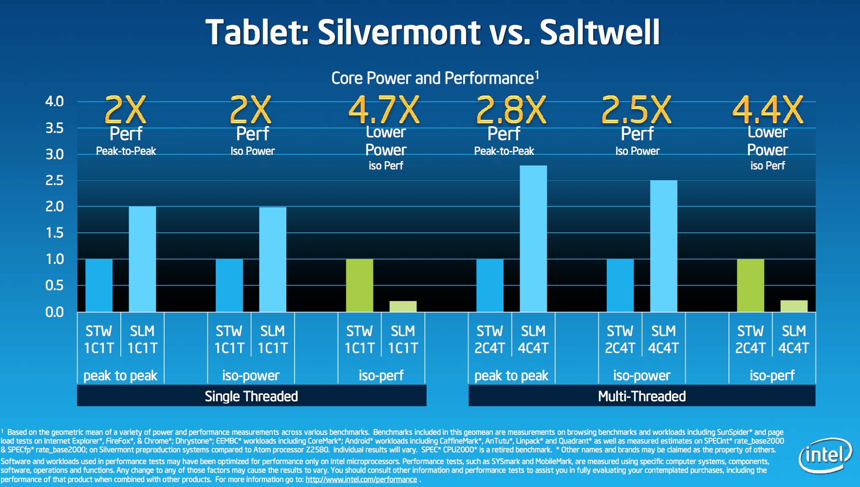
In terms of absolute performance, Silvermont’s peak single threaded performance is 2x that of Saltwell. This 2x gain includes IPC and clock frequency gains (only 50% is from IPC, the rest is due to IDI, system agent and frequency). Given that Saltwell is competitive with existing architectures from ARM and Qualcomm (except for the Cortex A15), a 2x increase in single threaded performance should put Silvermont in a leadership position when it arrives later this year.
The next set of bars is just as important. At the same power levels (Intel didn’t disclose specifically at what power), Silvermont delivers 2x the performance of Saltwell. Finally, at the same performance level, Silvermont uses 4.7x lower power. Given that Saltwell wasn’t terrible on power to begin with, this is very impressive. Without knowing the specific power and performance levels however, I wouldn’t draw too many conclusions based on this data though.
The multithreaded advantages are obviously even greater as Silvermont will be featured in quad-core configurations while Saltwell topped out at dual-core (4 threads) in tablets.
In the next two slides, Intel did some competitive analysis with Silvermont vs. the ARM based competition. The benchmarks are the same, but now we have specifics about power usage. In the first test Intel is comparing to three competitors all with quad-core designs. Intel claims to have estimated performance gains based on what is expected to be in the market by the end of this year. Intel’s performance modeling group is very good at what it does, but as with any estimate you always have to exercise some caution in buying the data until we have physical hardware in hand.
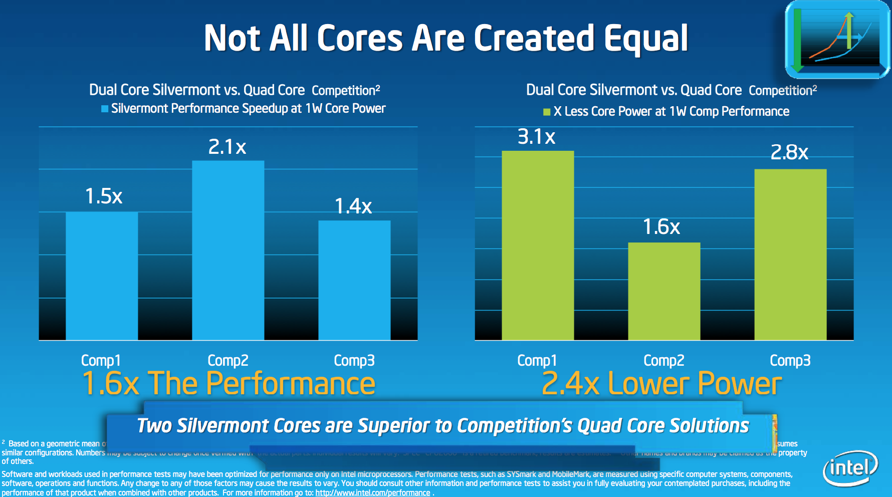
Intel isn’t naming the three competitors in this chart, but there are only a finite number of quad-core ARM players shipping in decent tablet designs these days. The chart on the left compares performance of a dual-core Silvermont to quad-core ARM based designs at a 1W core power level. This comparison is extremely important because it’s effectively demonstrating the type of advantage Intel hopes to have in smartphones next year.
The chart on the right fixes performance and shows the reduction in core power. Do keep in mind that there can be a big difference between core and device level power, although Intel does expect to be very competitive on battery life this round.
The final performance comparison slide increases max core power to 1.5W and compares quad-core Silvermont to the quad-core competition. You’ll note the arrival of a new competitor here. One of the bars is a dual-core SoC with its performance scaled to four cores. I’m less confident about that particular estimation simply because it assumes Apple won’t significantly update architectures in its next generation of iPads.
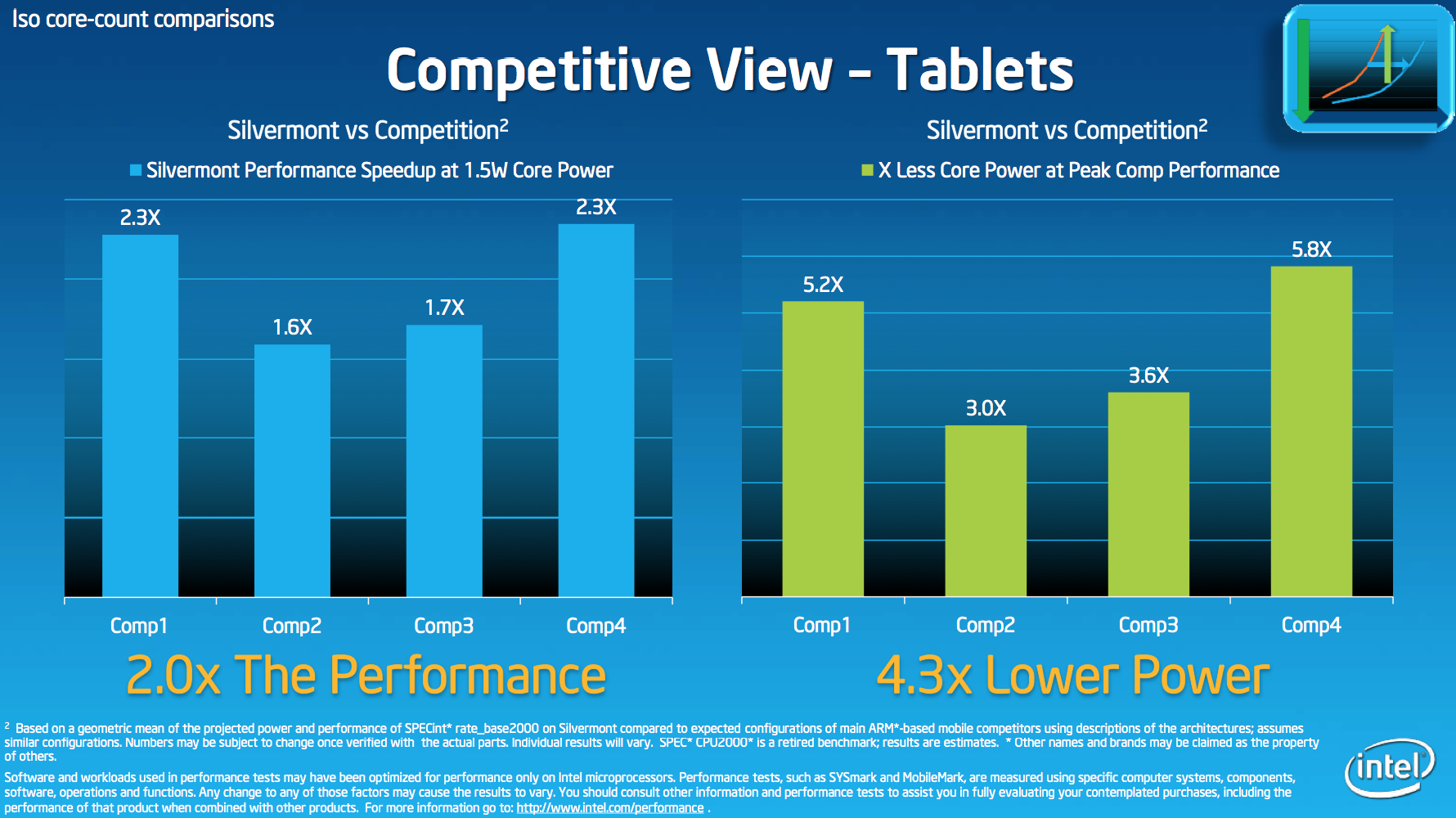
The performance deltas here are huge. If we assume that at least one of these bars represents a Cortex A15 based design, Silvermont looks very good.
That’s the end of the Intel data, but I have some thoughts to add. First of all, based on what I’ve seen and heard from third parties working on Baytrail designs - the performance claims of being 2x the speed of Clovertrail are valid. Compared to the two Cortex A15 designs I’ve tested (Exynos 5250, dual-core A15 @ 1.7GHz and Exynos 5410 quad-core A15 @ 1.6GHz), quad-core Silvermont also comes out way ahead. Intel’s claims of a 60% performance advantage, at minimum, compared to the quad-core competition seems spot on based on the numbers I’ve seen. Power is the only area that I can’t validate based on what I’ve seen already (no one has given me a Baytrail tablet to measure power on). Given what we know about Silvermont’s architecture and the gains offered by Intel’s 22nm process, I do expect this core to do better on power than what we’ve seen thus far from ARM’s Cortex A15.
There is something we aren’t taking into account though. As of now, the only Cortex A15 based SoCs that we’ve seen have been very leaky designs optimized for high frequency. Should an SoC vendor choose to optimize for power consumption instead, we could see a narrower gap between the power consumption of Cortex A15 and Silvermont. Obviously you give up performance when you do that, so it may not ultimately change anything - but the power story might be less of a blowout.
Final Words
Silvermont really is Intel’s Conroe for the mobile market, but not in the sense that many have been expecting. Given that success in mobile is so closely tied to device wins, Silvermont alone isn’t enough. Unlike Conroe, a very competitive Silvermont won’t change the world overnight. What Silvermont does however is offer a great foundation for Intel going forward. Conroe lead to Penryn, Nehalem, Westmere, Sandy Bridge, Ivy Bridge and soon, Haswell. It was the platform that Intel could build on regularly by executing on tick-tock. Conroe paved the way for the insane advantage Intel has held onto for the past few years. Silvermont is like Conroe in that it provides that same foundation.
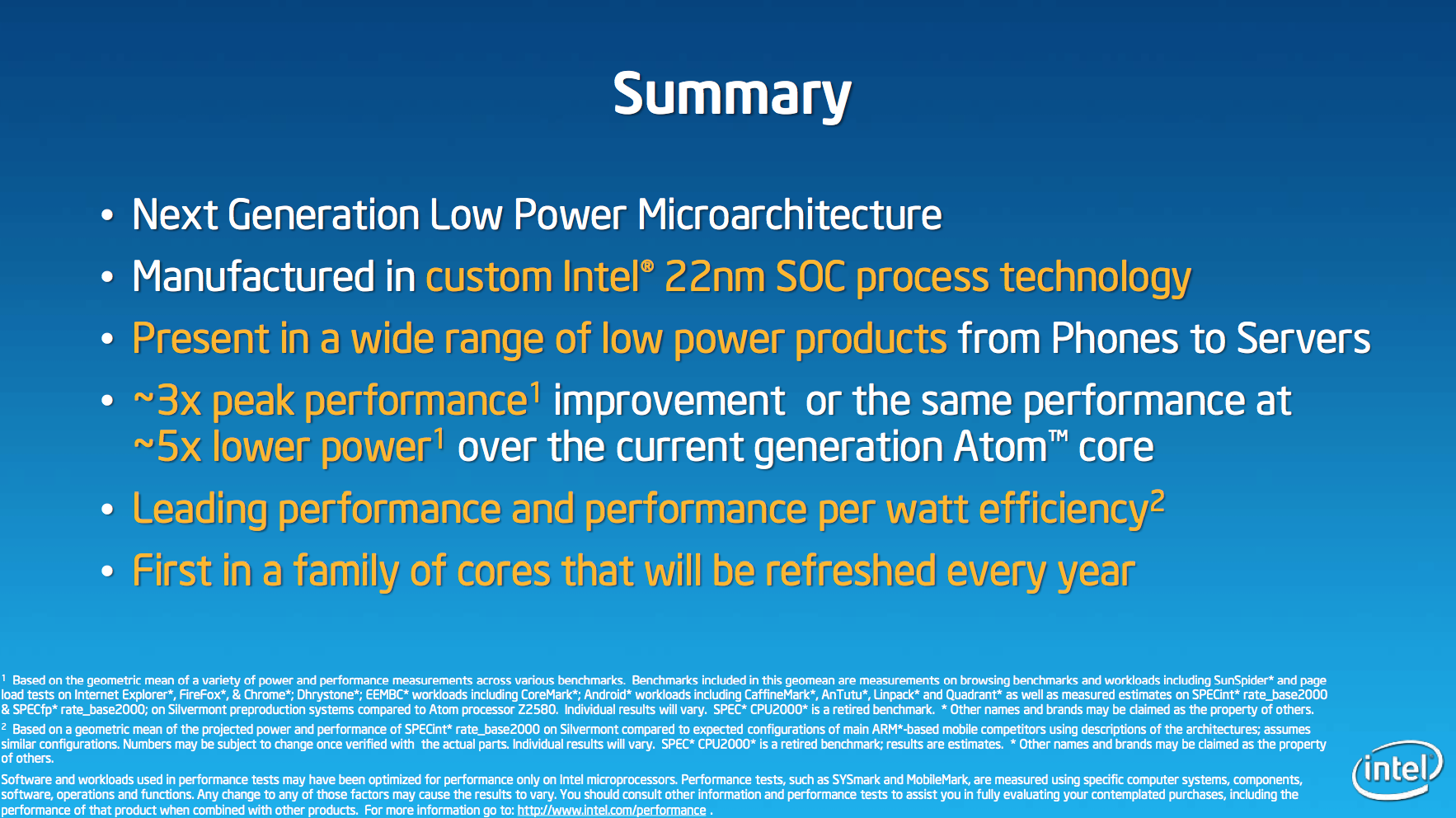
The mobile market is far more competitive than the PC industry was back when Conroe hit. There isn’t just one AMD but many competitors in the SoC space that are already very lean and fast moving. There’s also the fact that Intel doesn’t have tremendous marketshare in ultra mobile. Silvermont may feel a lot like Conroe, but the market it’s competing in is very different. That’s not to say that Intel can’t be successful here; it’s just not going to be easy.
Architecturally Silvermont is very conservative, and that’s not a bad thing. A side effect of not wanting to make Haswell irrelevant by a far lower cost part is the benefit of maintaining power efficiency. Intel joins the ranks of Apple and Qualcomm in intelligently scaling performance while respecting power consumption. Intel’s 22nm process should give Silvermont a lot of runway to use. If it can quickly follow up with 14nm, Silvermont’s power advantage could end up being akin to Conroe’s performance advantage in the mid-2000s.
Even so, Silvermont is long overdue. It’s the first mobile architecture where Intel really prioritized smartphones and tablets, and on paper, it looks very good. Now it’s up to Intel to turn a great architecture into great design wins. From what I’m hearing, we may actually see that happen.


